
Power Electronics
Course
Introduction to the
Fundamentals of Power
Electronics
PB-600
Student Lab
Manual

Power Electronics Course
PB-600
Student Lab Manual
Global Specialties
22820 Savi Ranch Parkway
Yorba Linda, CA 92887
www.globalspecialties.com
Published by Global Specialties
Yorba Linda, California
Copyright © 2022 by Global Specialties
All Rights Reserved. No part of this book shall be reproduced, stored in a retrieval system,
or transmitted by any means, electronic, mechanical, photocopying, recording, or otherwise,
without written permission from the publisher. No patent liability is assumed with respect to
the use of information contained herein. While every precaution has been taken in the
preparation of this book, the publisher assumes no responsibility for errors or omissions.
Neither is any liability assumed for damages resulting from the use of the information
contained herein.
451-069-001_rA
Power Electronics Student Lab Manual
5
Table of Contents
Introduction 7
Technical Specications 7
Panel Layout 8
About the Trainer 9
Operating Instructions 10
Answers (Pre-Lab) 80
List of Included Accessories 84
Power Electronics Student Lab Manual
6
Experiments
Experiment 1: Characteristics of an SCR 11
Experiment 2: Gate Control Characteristics of an SCR 13
Experiment 3: The UJT, Inter Base Resistance, and Intrinsic Standoff Ratio 15
Experiment 4: Characteristics of a MOSFET 17
Experiment 5: Characteristics of an IGBT 19
Experiment 6: Characteristics of a DIAC 21
Experiment 7: The IA - VA Characteristics of a TRIAC 23
Experiment 8: Characteristics of a PUT 26
Experiment 9: Class B Commutation Circuit 28
Experiment 10: Class C Commutation Circuit 30
Experiment 11: Class D Commutation Circuit 32
Experiment 12: Class F Commutation Circuit 34
Experiment 13: Resistor Triggering Circuit 36
Experiment 14: Resistor Capacitor Triggering Circuit (Half Wave) 38
Experiment 15: Resistor Capacitor Triggering Circuit (Full Wave) 40
Experiment 16: Triggering an SCR with a UJT 42
Experiment 17: Triggering an SCR with a IC-555 44
Experiment 18: Triggering an SCR with a IC-741 46
Experiment 19: RAMP and Pedestal Triggering Using Anti parallel SCR 48
Experiment 20: UJT Relaxation Oscillator 51
Experiment 21: Voltage Commutated Chopper 53
Experiment 22: Bedford Inverter 55
Experiment 23: Single Phase PWM Inverter with MOSFET 57
Experiment 24: Single Phase PWM Inverter with IGBT 59
Experiment 25: Half Wave Controlled Rectier with Resistive Load 61
Experiment 26: Half Wave Controlled Rectier with RL Load 63
Experiment 27: Full-Wave Controlled Rectier (Mid Point Conguration) with Resistive Load 65
Experiment 28: Full-Wave Controlled Rectier (Mid Point Conguration) with RL Load 68
Experiment 29: Fully Controlled Bridge Rectier with Resistive Load 70
Experiment 30: Fully Controlled Bridge Rectier with RL Load 72
Experiment 31: Low Side Buck Converter with Resistive Load 74
Experiment 32: Boost Converter with Resistive Load 76
Experiment 33: Buck-Boost Converter with Resistive Load 78

globalspecialties.com
Power Electronics Student Lab Manual
Introduction
The PB-600 provides a complete workstation for students to experiment with Power Electronics Circuits. Each
exercise, presented in the lab manual, guides the students with step-by-step procedures. These experiments
can be performed in the electronics laboratory of Colleges and Universities. It may also be utilized in Technical
Training centers as well. The intention is to better acquaint students with the characteristics of Power Electronics
devices and their applications. The Power Electronics Trainer will be benecial to Students majoring in
Engineering / Technology.
Technical Specications
Breadboard
1280 tie points and 4 Bus Strips with 100 tie points
each, totaling 1680 tie points. Size 112mm x 170mm
(Approx.)
DC Power Supply
± 5V at 100mA, ± 12V at 150mA, ± 15V at 50mA & ±
35V at 50mA
AC Power Supply
18V - 0V - 18V at 50mA, & 15V - 0V - 15V at 50mA
Triggering Circuit
5 gate signal output, Frequency range: 40Hz to 900Hz
Variable, Amplitude: 12V PWM control of G1, G2,
G3 and G4 Duty cycle control of “Gate” Signal is 0 to
100%
Single Phase Rectier
Firing Angle Control 0°-180° variables
Pulse Amplier
Firing Circuit Four gate signal output with isolation
transformer
SCR Assembly
2P4M (4 pieces) 600V, 2A
Power Devices
IGBT-G4BC20S;MOSFET-IRF540; UJT-2N2646,
DIAC-DB3; TRIAC-BT136; PUT- 2N6027; SCR-
TYN-612/02
Circuit Components
Capacitor: 0.01uF, 0.047uF, 0.1uF, 0.33uF, 1uF/63V (4
pieces), 2.2uF/50V
Diode: IN4007 (8 pieces), Zener Diode 9V, Inductor:
10mH, 68mH (2 pieces)
Resistor: 22Ω/5W, 100Ω/2W, 220Ω/2W, 10KΩ (3
pieces), 22KΩ, 33KΩ, 47KΩ,
Potentiometer
4.7KΩ (2 pieces), 1MΩ,
Load Resistance
120Ω, 270Ω, 1KΩ, 2.2KΩ, (Each 5W)
Pulse Transformer
1:1 (2 pieces), 1:1:1
Toggle Switch
SPDT
Power Requirements
115V ±6% 60Hz or 230V ±10%, 50Hz

Power Electronics Student Lab Manual
8
Panel Layout

globalspecialties.com
Power Electronics Student Lab Manual
About the Trainer
Block 01: DC Power Supply
Fixed DC output of +5V and -5V, +12V and -12V, +15V and -15V, +35V and -35V
Block 02: AC Power Supply
Fixed AC output of 18V-0V-18V and 15V-0V-15V
Block 03: Circuit Component
Diodes: IN4007 (8 pieces), Zener Diode 9V,
Capacitors: Cap 0.01 µF, Cap 0.047 µF, Cap 0.33 µF, Electrolytic Cap 1µF / 63V (4 pieces), 2.2µF / 63V
Resistors: 22Ω/5W, 100Ω/2W, 220Ω/2W, 10KΩ 0.25W (3 pieces), 22KΩ 0.25W, 33KΩ 0.25W, 47KΩ 0.25W
Inductors: 68mH (2 pieces), 10mH
Block 04: Power Devices
SCR TYN-612 (2 pieces), MOSFET IRF-540, IGBT- G4BC2OS, UJT 2N2646, PUT 2N 6027, DIAC DB-3, and
TRIAC BT-136
Block 5: Toggle Switch
Single Pole Double Throw (SPDT)
Block 6: Pulse Amplier & Isolation Transformer
This block provides amplication of gate signal, and it isolates the power circuit from the triggering circuit.
Block 7: Breadboard
840 X 2 Breadboard
Block 8: Triggering Circuit
(4) Gate Pulse with PWM Control and Frequency Control.
(1) “GATE” signal with Duty Cycle Control
Block 9: Load Selector, Resistive Load
Loads: 120 Ω /5W, 270 Ω /5W, 1K Ω /5W, 2.2K Ω /5W: with Load Selector
Block 10: Potentiometer
1MΩ and 4.7KΩ (2)
Block 11: SCR Assembly
SCR 2P4M Assembly (4 pieces)
Block 12: Single Phase Controlled Rectier Firing Circuit
(4) Gate and Cathode signal with isolation for single phase-controlled rectiers.
Block 13: Pulse Transformers:
Pulse Transformers for circuit isolation: (2) Transformers of 1:1 and (1) Transformer of 1:1:1.
WARNING:
Because of the potential hazard of working with electrical circuits, all proper precautionary measures should be
taken when operating this unit. Failure to do so could result in injury.
Power Electronics Student Lab Manual
10
Operating Instructions
The trainer contains an AC and DC power supply, with various voltages. The power supply is controlled by the
ON/OFF switch. When turned on, the LED on the ON/OFF switch will light up, indicating the power supply has
been activated.
The ‘TRIGGERING CIRCUIT” block, contains a Frequency, PWM, and Duty Cycle control.
The “FREQUENCY” control will vary the frequency of pulse signals G1, G2, G3, G4 and GATE. The “PWM
CONTROL” will vary the pulse width for inverter circuits. The “DUTY CYCLE” control will vary duty cycle of
“GATE” only.
In the “SINGLE PHASE CONTROLLED RECTIFIER FIRING CIRCUIT” block, the gate signals for two groups of
rectier devices. The ring angle is changed by rotating “FIRING ANGLE CONTROL POT”.
The “PULSE AMPLIFIER & ISOLATION TRANSFORMER” block can be used for Bedford inverter and series
inverter circuits.
The experiments presented in this manual are for guidance only. The trainees are expected to apply their
knowledge and skills to modify or correct any circuits wherever necessary. Pin diagrams, for the devices, are
provided at the end of the manual. Use them for proper connections.

globalspecialties.com
Power Electronics Student Lab Manual
Experiment 1:
Characteristics of an SCR
Introduction:
The Silicon-Controlled Rectier (SCR) is a common and crucial component in Power Electronics circuits. Like a
diode, the SCR has both an anode and cathode aspect to it. However, what distinguishes an SCR from a typical
diode is that it contains a gate input. The SCR will conduct in forward conduction mode if a high enough voltage is
applied across the anode and cathode. Forward conduction may also be achieved by applying a positive signal to
the gate. This lab will cover the voltage characteristics of an SCR and the forward conduction mode.
Pre-Lab Questions:
1. What is the main difference between an SCR and a typical Diode?
2. What is the P-N Conguration of an SCR, and where, in this P-N structure, is the Cathode, Anode, and
Gate connected?
3. A process referred to as doping is usually employed to control the number of charge carriers in a
semiconductor. What is this doping process, and why is it important in a P-N junction?
Apparatus Required: Quantity:
Resistance 510Ω, ¼ W 1
Resistance 2.2KΩ, 5W (on board) 1
SCR TYN 612 (on board) 1
Potentiometer 4.7KΩ (on board) 2
Multimeter 3
Patch Cord 10
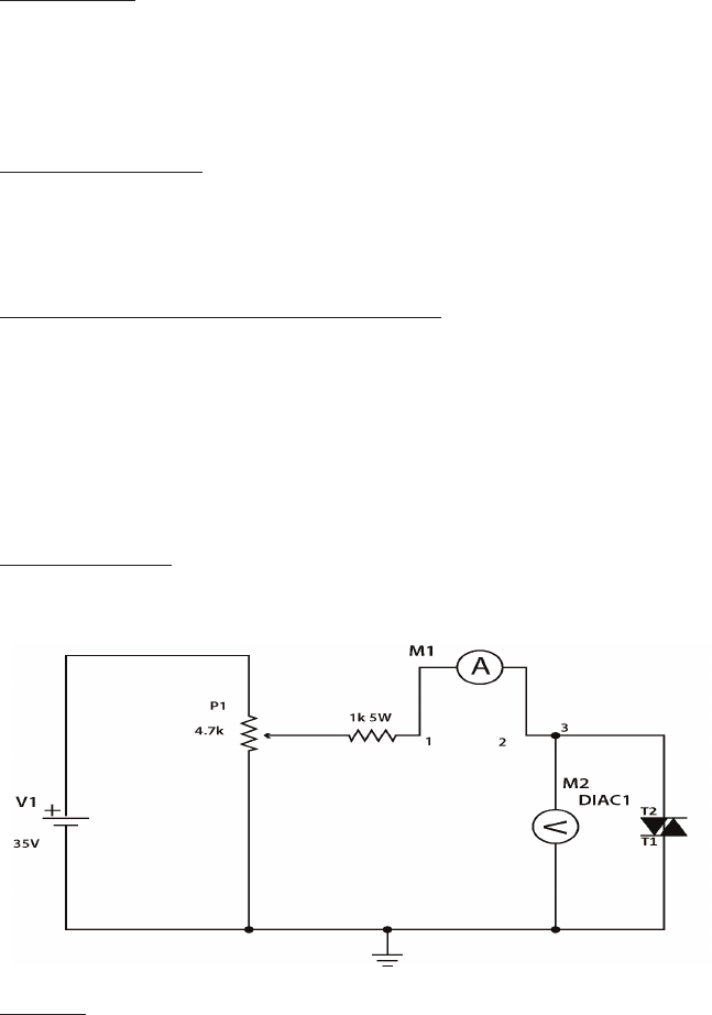
Circuit Diagram:
The circuit below can be used to plot the characteristics of an SCR.
Figure 1

Power Electronics Student Lab Manual
12
Procedure:
1. Connect the circuit as shown in Figure 1 using patch cords.
2. To plot the IA - VA characteristics proceed as follows.
3. Rotate potentiometer P1 and P2 in the full counterclockwise position. Connect the voltmeter at point ‘6’ &
ground to measure VG and at point ‘3’ & ground to measure VA.
4. Connect an ammeter between points ‘1’ & ‘2’ to measure the current IA and between points ‘4’ & ‘5’ to
measure the gate current IG.
5. Switch Power ON.
6. Set the gate current IG to a value between 3.75mA - 3.85mA, by varying potentiometer P2.
7. Gradually increase anode voltage VA, by varying potentiometer P1.
8. Observe current IA, it should read near zero initially.
9. At some point, the positive anode current IA will have a sudden jump in reading. When this occurs, the
voltmeter reading will drop to near zero. This will indicate the ring of the SCR.
10. If this does not occur, repeat steps 5 - 8 with a slightly higher gate current IG value set.
11. As VA is being increased, record the observed voltage VA and corresponding current IA values on the table
provided.
12. After the ring of the SCR, continue to increase VA, and record the observed VA and corresponding IA
values.
13. Use the recorded values to plot and graph the IA vs VA curve.
Table 1: SCR Measured Values:
IA
Gate Current I
G
= __________mA
Voltage V
A
and Current I
A
(mA)
1
VA
No.
2
3
4
5
6
7
8
9
10
Image 1: SCR I vs V Curve

globalspecialties.com
Power Electronics Student Lab Manual
Experiment 2:
Gate Control Characteristics of an SCR
Introduction:
An SCR is like a diode, but the SCR has an added gate control to it. Sending a pulse through the gate of the SCR
will enable it to enter forward conduction mode. While the gate remains positive the SCR can conduct current in
the forward conduction mode. This lab covers how an SCR turns on and off by controlling the gate input.
Pre-Lab Questions:
1. What are two methods that will generate forward conduction in an SCR?
2. What is Breakover Voltage in an SCR?
3. What is the holding current in an SCR?
Apparatus Required: Quantity
Resistance 510Ω, ¼ W 1
Resistance 2.2KΩ, 5W (on board) 1
SCR TYN 612 (on board) 1
Potentiometer 4.7KΩ (on board) 2
Multimeter 4
Patch Cord 16
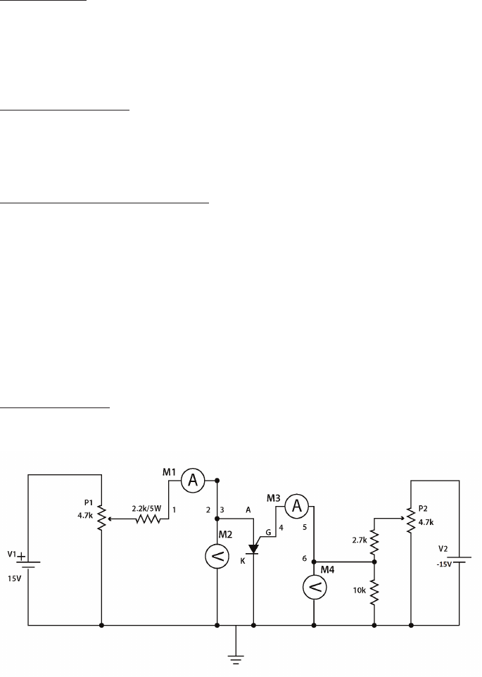
Circuit Diagram:
The circuit below can be used to plot the characteristics of an SCR.
Figure 2

Power Electronics Student Lab Manual
14
Procedure:
1. Connect the circuit as shown in Figure 2 using patch cords.
2. To plot the IG - VA characteristics proceed as follows.
3. Rotate potentiometer P1 and P2 in the full counterclockwise position. Connect voltmeter at point ‘6’ &
ground to measure VG and at point ‘3’ & ground to measure VA.
4. Connect ammeter between points ‘1’ & ‘2’ to measure the current IA and between points ‘4’ & ‘5’ to measure
the gate current IG.
5. Switch Power ON.
6. Set voltage VA to 5V by varying potentiometer P1.
7. Gradually increase the gate current IG until the SCR is triggered. A sudden increase in the measured IA and
a drop, to a near zero reading, in the measured VA, is an indication that the SCR has red on.
8. On the table provided, record the measured current IG value at which the SCR is triggered.
9. After the ring of the SCR, continue to increase the gate current IG and observe whether it has any effect
on IA or VA.
10. Increase VA by increments of 5V and repeat steps 5 – 8. Continue this process until a minimum of ve
points, to plot, have been acquired.
11. Plot and graph the IG vs VA curve.
Table 2: SCR Measured Values
I
G
No.
Voltage V
A
and Gate Current I
G
(mA)
1
V
A
2
3
4
5
6
7
8
9
10

globalspecialties.com
Power Electronics Student Lab Manual
Experiment 3:
The UJT, Inter Base Resistance, and Intrinsic Standoff
Ratio
Introduction:
A unijunction transistor (UJT) is a unique three terminal semiconductor device. When the UJT is triggered, the
emitter current increases until limited by the emitter power supply. It can be used in switching pulse generators,
and as a triggering device for an SCR or TRIAC. This lab will cover the characteristics of the UJT to nd the inter
base resistance as well as the intrinsic standoff ratio. This is done by observing the change in emitter current.
Pre-Lab Questions:
What is the UJT physical structure with respect to P-type and N-type material?
In what way will applying positive voltage to the emitter affect the total resistance between base 1 and base 2?
What is the inter-base resistance and the intrinsic stand-off ratio?
Apparatus Required: Quantity
Resistance 510 Ω ¼ W 2
Potentiometer 4.7K (on board) 2
UJT 2N2646 (on board) 1
Multimeter 3
Patch Cord 9
Circuit Diagram:
The circuit below can be used to plot the characteristics of a Unijunction Transistor.
Figure 3
Procedure:
1. Connect the circuit as shown in Figure 3 using patch cords.
2. To plot the Emitter characteristics, proceed as follows:
3. Rotate potentiometer P1 and P2 in the full counterclockwise position.
4. Connect the voltmeter at point ‘6’ and ground to read VBB and at point ‘3’ and ground to read VE.
5. Connect ammeter between points ‘1’ and ‘2’ to measure the emitter current IE, and between points ‘4’ and
‘5’ to measure the base current IB.
6. Switch Power ON.
7. Vary potentiometer P2 and set a voltage value of VBB = 5V.
8. Increase the Emitter voltage VE in steps.
9. Continue to increase VE until the reading on the voltmeter drops. At this point the UJT res on and emitter

Power Electronics Student Lab Manual
16
current will ow rapidly.
10. In Table 3, record the Emitter voltage VE and the corresponding Emitter current IE for each observation
value.
11. Repeat steps 4 through 8 for VBB = 10V and VBB = 15V.
12. Plot the VE vs IE graph with the observation values recorded on table 3.
Table 3: UJT Measured Values
V
E
I
E
V
E
I
E
V
E
I
E
10
1
2
3
4
5
6
7
8
9
No.
V
BB
= 10V
V
BB
= 15V
Emitter Voltage V
E
and Emitter Current I
E
(mA)
V
BB
= 5V
Image 3: UJT V vs I Curve
Calculations:
Inter base Resistance (RBB)It is the sum of resistance between base 1 & base 2
RBB = RB1 + RB2
It ranges from 4K to 10K ohms when IE = 0.
Intrinsic stand-off Ratio (η)
η = R B1 / (R B1+R B2) = RB B1 / RBB
It ranges from 0.51 to 0.82.

globalspecialties.com
Power Electronics Student Lab Manual
Experiment 4:
Characteristics of a MOSFET
Introduction:
The Metal Oxide Semiconductor Field Effect Transistor (MOSFET) is a device used in a variety of different
circuits. Because of its small compact size, it is used as a switch in analog and digital circuits. It is a four terminal
device consisting of a source, gate, drain and base terminal. The base and source are usually connected, so the
MOSFET operates as a three-terminal transistor. This lab will cover the characteristics of a MOSFET device with
a focus on the voltage and current plots.
Pre-Lab Questions:
MOSFET is an acronym for Metal Oxide Semiconductor Field Effect Transistor. Why is it considered a eld effect
transistor? What makes it different from an SCR or UJT?
According to the MOSFET circuit symbol printed on the face of the Trainer, Is this MOSFET an N-channel or
P-channel?
What is the P-N structure of the MOSFET, used in this lab?
Apparatus Required: Quantity
Resistance 820Ω, ¼ W 1
Resistance 1KΩ, 5W (on board) 1
Resistance 510Ω, ¼ W 1
Zener diode 9V (on board) 1
Potentiometer 4.7KΩ (on board) 2
MOSFET IRF540N (on board) 1
Multimeter 3
Patch Cord 14
Circuit Diagram:
The circuit below can be used to plot the characteristics of a MOSFET
Figure 4

Power Electronics Student Lab Manual
18
Procedure:
1. Connect the circuit as shown in Figure 4 using patch cords.
2. To plot the ID vs VDS characteristics, proceed as follows:
3. Connect the circuit using the breadboard
4. Rotate potentiometer P1 and P2 in the full counterclockwise position.
5. Connect an ammeter between points ‘1’ and ‘2’ and connect a second ammeter between points ‘4’ and ‘5’.
6. Connect a voltmeter at point ‘6’ and ground to measure drain voltage VDS. Connect voltmeter at point ‘3’
and ground to measure gate voltage VGS.
7. Switch Power ON
8. Vary potentiometer P1 and set the gate voltage VGS at some constant value (2.5V, 2.6V, 2.7V)
9. Increase the drain voltage VDS value from 0 to 35V in steps by varying potentiometer P2. In Table 4,
record the measured Drain voltage VDS and corresponding Drain current ID values, with the constant Gate
voltage VGS set.
10. Rotate potentiometer P2 in the full counterclockwise position.
11. Repeat steps 1 through 6 with a different gate voltage VGS value set.
12. Plot and graph the ID vs VDS curve using the recorded measured values, appropriately scaled. The graph
will produce the Drain characteristics curve for a MOSFET.
Table 4: Observations
V
DS
I
D
V
DS
I
D
V
DS
I
D
No.
V
GS
= _______
V
GS
= _______
Voltage V
D
and Current I
D
(mA)
V
GS
= _______
10
1
2
3
4
5
6
7
8
9
Image 4: MOSFET I vs V Curve

globalspecialties.com
Power Electronics Student Lab Manual
Experiment 5:
Characteristics of an IGBT
Introduction:
The Insulated Gate Bipolar Transistor (IGBT) is a three terminal semiconductor device. Like a MOSFET, it can
operate as a switch due to its high efciency and fast switching capabilities. The IGBT is used in many high-
power applications such as electric cars, variable frequency drives and refrigerator units. This lab will cover the
characteristics of an IGBT device, with a focus on voltage and current plots.
Pre-Lab Questions:
How will increasing the gate current affect the current ow through the IGBT?
According to the provided Data Sheet, what is the maximum voltage VCES that should be applied across the
IGBT, being used in this experiment?
Apparatus Required: Quantity
Resistance 22Ω, 5W (on board) 1
Resistance 1KΩ, ¼ W 1
Potentiometer 4.7KΩ (on board) 2
IGBT G4BC20S (on board) 1
Multimeter 3
Patch Cord 11
Circuit Diagram:
The circuit below can be used to plot the characteristics of an IGBT.
Figure 5
Procedure:
1. Connect the circuit as shown in Figure 5 using patch cords.
2. Rotate the potentiometer P1 in the full clockwise position and P2 in the full counterclockwise position.
3. Connect the rst ammeter between points ‘4’ and ‘5’ to measure Collector current IC (mA).
4. Connect the second ammeter between points ‘1’ and ‘2’.
5. Connect voltmeter at point ‘3’ and ground to measure the Gate voltage VGE and at point ‘6’ and ground to

Power Electronics Student Lab Manual
20
measure Collector voltage VCE.
6. Switch Power ON.
7. Vary the potentiometer P1 to set the gate voltage VGE between 4.8Vand 5.4V.
8. Vary the potentiometer P2 to increase the value of Collector-Emitter voltage VCE from 0 to 35V in steps.
In Table 5, record the Collector-Emitter voltage VCE and the corresponding Collector current IC for each
measured value observed.
9. Rotate the potentiometer P2 in the full counterclockwise position and potentiometer P1 in the full clockwise
position.
10. Repeat steps 1 through 6 with a different gate voltage VGE set.
11. Plot and graph the IC vs VCE curve using the measured values, appropriately scaled. The curve depicts the
IGBT characteristics.
Table 5: IGBT Measured Values
V
CE
I
C
V
CE
I
C
No.
V
GE = _______
V
GE = _______
Voltage VCE and Current IC (mA)
10
1
2
3
4
5
6
7
8
9
Image 5: IGBT I vs V Curve
globalspecialties.com
Power Electronics Student Lab Manual
Experiment 6:
Characteristics of a DIAC
Introduction:
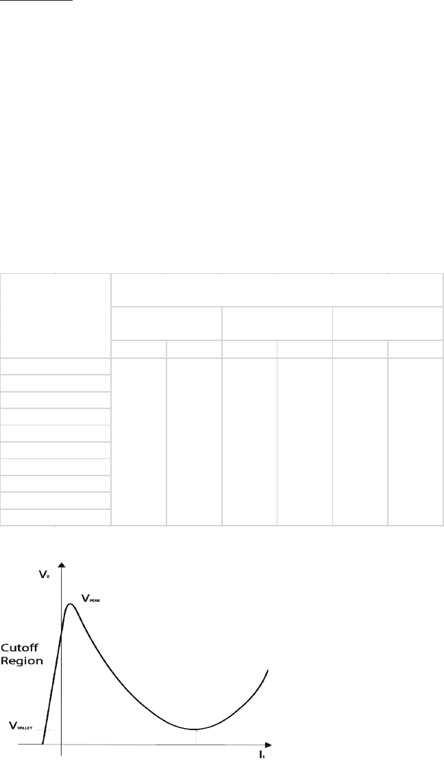
The Diode for Alternating Current (DIAC) is a diode that conducts after its breakover voltage has been met. After
this, the DIAC experiences a drop in voltage with an increase in current. It is a bidirectional device and sometimes
referred to as a symmetrical trigger diode due to its I-V characteristics. This lab will cover the characteristics of a
DIAC and show the symmetrical relationship mentioned.
Pre-Lab Questions:
1. What distinguishes a DIAC from an ordinary diode?
2. What is the DIAC circuit symbol?
3. What is the typical breakover voltage for the DIAC used in this lab?
Apparatus Required: Quantity
Resistance 1KΩ, 5W (on board) 1
DIAC DB3 (on board) 1
Potentiometer 4.7KΩ (on board) 1
Multimeter 2
Patch Cord 6
Circuit Diagram:
The circuit below can be used to plot the characteristics of a DIAC.
Figure 6

Power Electronics Student Lab Manual
22
Procedure:
1. Connect the circuit, as shown in Figure 6, using patch cords.
2. To plot the IA-VA characteristics proceed as follows.
3. Rotate potentiometer P1 in the full counterclockwise position.
4. Connect voltmeter at point ‘3’ & ground to read voltage VA.
5. Connect ammeter between points ‘1’ & ‘2’ to measure current IA.
6. Connect the circuit to +35V.
7. Switch Power ON
8. Increase DIAC voltage VA by varying the potentiometer P1. In Table 6, record the observed measured
voltage values VA and the corresponding current values IA.
9. Rotate potentiometer P1 in the full counterclockwise position.
10. Switch Power OFF
11. Connect the circuit to -35V.
12. Switch Power ON.
13. Increase DIAC voltage VA by varying the potentiometer P1. In Table 6, record the observed measured
voltage values VA and the corresponding current values IA.
14. Plot and graph the IA vs VA curve for both the +35V circuit and -35V circuit.
Table 6: DIAC Measured Values
V
A
I
A
V
A
I
A
1
DIAC Voltage VA and Current IA (mA)
No.
2
3
4
5
6
7
8
9
10
Image 6: DIAC I vs V Curve

globalspecialties.com
Power Electronics Student Lab Manual
Experiment 7:
The IA - VA Characteristics of a TRIAC
Introduction:
The Triode for Alternating Current (TRIAC) is a three terminal component able to conduct current in both
directions, when the gate is triggered. A TRIAC is composed of a thyristor which makes it similar to an SCR.
However, an SCR can only conduct current in one direction. A TRIAC can function as a switch for alternating
current. Lamp dimming, motor control, and electric heaters are just a few of its applications. This lab will cover the
IA-VA characteristics of a TRIAC and show the bidirectional current control.
Pre-Lab Questions:
1. How are a TRIAC and a DIAC alike?
2. How are they different?
Apparatus Required: Quantity
Resistance 510Ω, ¼ W 1
Resistance 2.2KΩ, 5W (on board) 1
TRIAC BT136 (on board) 1
Potentiometer 4.7KΩ (on board) 2
Multimeter 4
Patch Cord 10
Circuit Diagram:
The circuit below can be used to plot the characteristics of a TRIAC.
Figure 7

Power Electronics Student Lab Manual
24
Procedure:
1. Connect the circuit, as shown in Figure 7, using patch cords.
2. To plot the IA-VA characteristics proceed as follows:
3. Rotate potentiometer P1 in the full counterclockwise position and P2 in the full clockwise position.
4. Connect voltmeter at point ‘6’ and ground to measure VG and at point ‘3’ and ground to measure VA.
5. Connect one ammeter between points ‘1’ & ‘2’ to measure current IA. Connect a second ammeter between
points ‘4’ & ‘5’ to measure gate current IG.
6. Connect circuit to +35V.
7. Switch Power ON
8. Vary potentiometer P2 to set the gate current IG to a value between 0 - .5mA.
9. Increase anode voltage VA gradually by varying potentiometer P1.
10. Observe the current IA in the anode circuit. In the initial stage the measured value is nearly zero.
11. If this does not happen, repeat the steps 8 through 10 with a slightly higher gate current IG set.
12. Experiment with different Gate current values to re up the TRIAC.
13. When the TRIAC res on, record the measured VA voltage value and the corresponding measured IA
current value in Table 7.
14. Rotate potentiometer P1 in the full counterclockwise position.
15. Connect the circuit to -35V and repeat from steps 7 through 13 and record the measured values on Table
7A.
16. Plot and graph the IA vs VA curve for both +35V circuit and -35V circuit.
Table 7A: TRIAC Measured Values (+35V)
VA IA VA IA VA IA
Voltage V
A
and Current I
A
(mA)
10
1
2
3
4
5
6
7
8
9
No.
I
G
= _______
I
G
= _______
I
G
= _______

globalspecialties.com
Power Electronics Student Lab Manual
Table 7B: TRIAC Measured Values (-35V)
V
A
I
A
V
A
I
A
V
A
I
A
Voltage V
A
and Current I
A
(mA)
10
1
2
3
4
5
6
7
8
9
No.
I
G
= _______
I
G
= _______
I
G
= _______
Image 7: TRIAC I vs V Curve
Power Electronics Student Lab Manual
26
Experiment 8:
Characteristics of a PUT
Introduction:
The Programmable Unijunction Transistor (PUT) is a three-terminal component, like a UJT. However, in a PUT
the peak voltage and intrinsic standoff ratio can be controlled using external resistors. A PUT is used for relaxation
oscillators, thyristor ring, and timing circuits. This lab will cover the characteristics of a PUT, and it will go over
how the voltage peak and intrinsic standoff ratio can be programmed.
Pre-Lab Questions:
1. What is the mathematical formula to determine the peak voltage of a PUT?
2. Given the predetermined gate voltage, for this lab, what should be the peak voltages for each run?
3. Looking at the circuit for this lab experiment, explain how the resistors control the peak voltage?
Apparatus Required: Quantity
Resistance 2.7KΩ, ¼ W 1
Resistance 10KΩ, ¼ W (on board) 1
Resistance 2.2KΩ, 5W (on board) 1
PUT 2N 6027 (on board) 1
Potentiometer 4.7KΩ (on board) 2
Multimeter 3
Patch Cord 14
Circuit Diagram:
The circuit below can be used to plot the characteristics of a PUT.
Figure 8
globalspecialties.com
Power Electronics Student Lab Manual
Procedure:
1. Connect the circuit, as shown in Figure 8, using patch cords.
2. To plot the PUT characteristics proceed as follows:
3. Rotate potentiometers P1 and P2 in the full clockwise position.
4. Connect the rst ammeter between points ‘1’ and ‘2’ to measure Anode current IA (mA). Connect the
second ammeter between points ‘4’ and ‘5’ to measure Gate current Ig (mA).
5. Connect voltmeter at point ‘3’ and ground to measure the Anode voltage VA.
6. Connect voltmeter at point ‘6’ and ground to measure the Gate voltage VG.
7. Switch Power ON.
8. Vary potentiometer P2 to set Gate voltage VG to a constant value (2.0V, 5.0V, 10V).
9. Vary potentiometer P1 to increase the anode voltage VA from 0 to 15V in steps. In Table 8, record the
measured Anode voltage VA value and corresponding Anode current IA value at each step.
10. Rotate potentiometer P2 in the full counterclockwise position.
11. Set the Gate voltage VG to a different value and repeat steps 6 through 7.
12. Plot and graph the VA vs IA curve.
Table 8: PUT Measured Values
V
A
I
A
V
A
I
A
V
A
I
A
Voltage V
A and Current IA (mA)
10
1
2
3
4
5
6
7
8
9
No.
VG = _______
VG = _______
VG = _______
Image 8: PUT V vs I Curve

Power Electronics Student Lab Manual
28
Experiment 9:
Class B Commutation Circuit
Introduction:
Commutation is the process of shutting off an SCR. This process is done by reducing the forward current to zero.
There are three different types of commutation methods natural, forced, and dynamic. Class B commutation is
considered forced commutation. It is commonly used in chopper and inverter circuits. The inductor and capacitor,
connected in parallel with the SCR, create a resonant pulse commutation. This lab will cover shutting off an SCR
by means of a Class B commutation circuit setup.
Pre-Lab Questions:
As mentioned, commutation is the process of turning off an SCR. Explain how this process is achieved in this
circuit, after the SCR is triggered?
Apparatus Required: Quantity
Resistance 1K, ¼ W 1
Electrolytic capacitor 2.2uF/63V (on board) 1
Inductor 10mH (on board) 1
SCR 2P4M (on board) 1
Patch cord 6
Circuit Diagram:
The class B commutation circuit diagram is shown below:
Figure 9

globalspecialties.com
Power Electronics Student Lab Manual
Procedure:
1. Connect circuit as shown in Figure 9.
2. Connect Gate of SCR to G1 signal, in the “TRIGGERING CIRCUIT” block.
3. Switch on the LAB.
4. Adjust “PWM CONTROL” to pulse the gate.
5. Connect oscilloscope across SCR and observe the waveform.
6. Connect oscilloscope across load resistance and observe waveform.
Image 9: Class B Commutation Waveform

Power Electronics Student Lab Manual
30
Experiment 10:
Class C Commutation Circuit
Introduction:
The class C commutation circuit is considered forced commutation. It differs from class B in that it utilizes two
SCRs connected in parallel. The class C circuit is referred to as complementary commutation. The circuit consists
of a main SCR and an auxiliary SCR. When the main SCR is turned on the capacitor connecting them charges to
peak value. When this occurs, the auxiliary SCR will turn on, shutting off the rst SCR. This process will continue
to repeat while the circuit is powered. This lab will cover the mentioned effect by using an oscilloscope to view the
output at both SCRs.
Pre-Lab Questions:
Both Class B and Class C are considered forced commutation. However, Class C utilizes two SCRs. Explain how,
in the circuit for this lab, resonant current will shut off both SCR, once they are triggered?
Apparatus Required: Quantity
Resistance 2.7KΩ, ¼ W 2
CAP. 0.1 MFD (on board) 1
SCR TYN 612 (on board) 2
Patch cord 10
Circuit Diagram:
The class C commutation circuit diagram is shown below:
Figure 10

globalspecialties.com
Power Electronics Student Lab Manual
Procedure:
1. Connect the circuit as shown in Fig. 10.
2. Connect G1 & G2 signal to gate of SCR.
3. Switch Power ON.
4. Connect Oscilloscope across SCR and observe waveform.
5. Connect oscilloscope across load resistance and observe waveform.
Image 10: Class C Commutation Waveform

Power Electronics Student Lab Manual
32
Experiment 11:
Class D Commutation Circuit
Introduction:
The class D commutation circuit is also considered forced commutation. Like class C, the class D circuit consists
of a main SCR and an auxiliary SCR. Class D, however, has an added diode and inductor connected in parallel
with the main SCR. It is commonly referred to as impulse commutation or voltage commutation due to the
waveforms of the SCRs. This lab will cover the characteristics of a class D commutation circuit by using an
oscilloscope to view the output at both SCRs.
Pre-Lab Questions:
In Class C commutation, SCR1 shuts off whenever SCR2 is triggered and vice versa. Does the same process
apply in Class D commutation? Why?
Apparatus Required: Quantity
Resistance 510Ω, ¼ W 1
Met. Cap 0.33 MFD (on board) 1
SCR 2P4M (on board) 2
Inductor 68mH (on board) 1
Diode IN4007 (on board) 1
Patch cord 10
Circuit Diagram:
The class D commutation circuit diagram is shown below:
Figure 11

globalspecialties.com
Power Electronics Student Lab Manual
Procedure:
1. Connect the circuit as shown in Fig. 11.
2. Connect G1 & G2 signal to gate of SCR1 & SCR2.
3. Switch Power ON.
4. Connect oscilloscope across SCR1 & SCR2 and observe waveforms.
5. Connect oscilloscope across Load and observe waveforms.
Image 11: Class D Commutation Waveform

Power Electronics Student Lab Manual
34
Experiment 12:
Class F Commutation Circuit
Introduction:
The class F commutation circuit is considered natural commutation, also known as source or line commutation.
In class F commutation, the SCR is switched on and off by the voltage source and not the circuit components.
An AC supply source is used to turn off the SCR at the end of every positive cycle. The class F circuit is used in
commutated inverters, controlled rectiers and cycloconverters. This lab will cover the characteristics of the class
F commutation circuit by using an oscilloscope to view the output of the SCR.
Pre-Lab Questions:
The Class F commutation circuit is much simpler than the previous ones that have been presented. It consists of
a power source, SCR, and load. How is the SCR shut off in this circuit, after it has been triggered on?
Apparatus Required: Quantity
Resistance 1KΩ, 5W (on board) 1
SCR 2P4M (on board) 1
Patch cord 5
Circuit Diagram:
The class F commutation circuit diagram is shown below:
Figure 12

globalspecialties.com
Power Electronics Student Lab Manual
Procedure:
1. Connect the circuit, as shown in Figure 12, using patch cords.
2. Connect GR1 signal to Gate of SCR.
3. Switch Power ON
4. Vary the Firing Control Pot and observe waveform across Load.
5. Vary the Firing Control Pot and observe waveform across the SCR
Image 12: Class F Commutation Waveform

Power Electronics Student Lab Manual
36
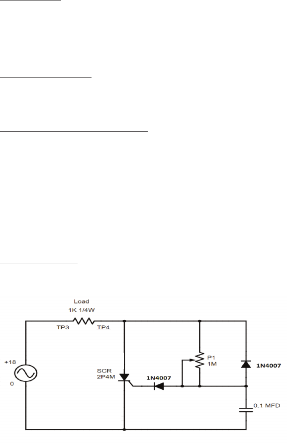
Experiment 13:
Resistor Triggering Circuit
Introduction:
The resistor triggering circuit is used to control the SCR over a 90° range. The resistors and diodes connected
in this circuit act as a gate control to trigger the SCR. It is the simplest resistor triggering circuit, but it has many
disadvantages. The circuit is very inefcient and leads to huge power losses. Resistors are very bulky in size and
take up a lot of room on circuit boards. This circuit is useful to understand simple triggering of an SCR before
moving on to a more complex circuit. This lab will cover the characteristics of a resistor triggering circuit by using
an oscilloscope to view the output of the SCR.
Pre-Lab Questions:
1. How does the Potentiometer control the triggering of the SCR?
2. Why is the ring angle control limited to 90°?
Apparatus Required: Quantity
Resistance 1KΩ, ¼ W 1
Resistance 510Ω, ¼ W 2
Potentiometer 1MΩ (on board) 1
SCR 2P4M (on board) 1
Diode IN4007 (on board) 1
Patch cord 10
Circuit Diagram:
The SCR Resistor Triggering Circuit diagram is shown below:
Figure 13

globalspecialties.com
Power Electronics Student Lab Manual
Procedure:
1. Connect the circuit, as shown in Figure 13, using patch cords.
2. Rotate potentiometer P1 in the full clockwise position.
3. Switch Power ON.
4. Connect the oscilloscope CH1 across the load and observe the phase angle and voltage.
5. Now, connect the oscilloscope across the thyristor and observe the waveform.
6. To see the phase angle variation, slowly vary the potentiometer.
7. Repeat the experiment from step 5 for various angles and plot the graphs by T = (α x 10ms)/180.
Table 13: Observed Values
1
No.
Load Voltage (V)
Phase Angle (α)
2
3
4
5
6
7
8
9
10
Image 13: Waveforms of R ring circuit
Power Electronics Student Lab Manual
38
Experiment 14:
Resistor Capacitor Triggering Circuit (Half Wave)
Introduction:
The resistor capacitor triggering circuit, half wave, is used to control the SCR over the entire 180° range. This
circuit differs from the previous one in that it has an additional diode and capacitor in the circuit. This circuit
produces a half wave, on the positive side of the waveform. This is due to the additional diode blocking the
negative direction of current ow resulting in a half wave circuit.
Pre-Lab Questions:
Both Resistor triggering and resistor capacitor triggering circuits have a similar wave form for voltage across the
SCR. What is the major difference between these two circuits?
Apparatus Required: Quantity
Resistance 1KΩ, ¼ W 1
Potentiometer 1MΩ (on board) 1
SCR 2P4M (on board) 1
Diode IN4007 (on board) 2
Met. Cap. 0.1 MFD (on board) 1
Patch cord 11
Circuit Diagram:
The Resistor Capacitor Triggering Circuit (Half Wave) diagram is shown below:
Figure 14

globalspecialties.com
Power Electronics Student Lab Manual
Procedure:
1. Connect the circuit, as shown in Figure 14, using patch cords.
2. Rotate potentiometers P1 in the full counterclockwise position.
3. Switch Power ON.
4. Connect the Oscilloscope probe across the Load and observe the phase angle and voltage.
5. Now, connect the oscilloscope probe across the thyristor and observe the waveform.
6. Vary the potentiometer slowly to see the phase angle variation.
7. Repeat the experiment from step 5 for various angles and plot the graphs. T = (α x 10ms)/180
Table 14: Observed Values
1
No.
Load Voltage (V)
Phase Angle (α)
2
3
4
5
6
7
8
9
10
Image 14: RC Half Wave Firing Circuit Waveform

Power Electronics Student Lab Manual
40
Experiment 15:
Resistor Capacitor Triggering Circuit (Full Wave)
Introduction:
The resistor capacitor triggering circuit, full wave, is used to control an SCR over the entire 180° range while
triggering negative side voltage waveforms. This circuit is very similar to the halfwave with the main difference
being the additional diodes at the source voltage which allow the circuit to conduct over the entire cycle. This lab
will cover the characteristics of the full wave circuit by using an oscilloscope to look at the waveform obtained at
the output of the SCR.
Pre-Lab Questions:
How will varying potentiometer P1 affect the triggering phase angle?
Apparatus Required: Quantity
Resistance 510Ω, ¼ W 1
Resistance 1KΩ, 5W (on board) 1
SCR 2P4M (on board) 1
Potentiometer 1MΩ (on board) 1
Ele. Cap 1MFD (on board) 1
Diode IN4007 (on board) 4
Patch cord 15
Circuit Diagram:
The Resistor Capacitor Triggering Circuit (Full Wave) diagram is shown below:
Figure 15
Procedure:

globalspecialties.com
Power Electronics Student Lab Manual
1. Connect the circuit, as shown in Figure 15, using patch cords.
2. Rotate potentiometer P1 in the full clockwise position.
3. Switch Power ON.
4. Connect the oscilloscope probe across the 510Ω resistor, observe the phase angle and voltage.
5. Now, connect the oscilloscope probe across the thyristor, observe the waveform.
6. Vary the potentiometer slowly to see the phase angle variation.
7. Repeat the experiment from step 5 for various angles and plot the graphs. T = (α X 10ms) / 180
Table 15: Observed Values
1
No.
Load Voltage (V)
Phase Angle (α)
2
3
4
5
6
7
8
9
10
Image 15: RC Full Wave Firing Circuit Waveform
Power Electronics Student Lab Manual
42
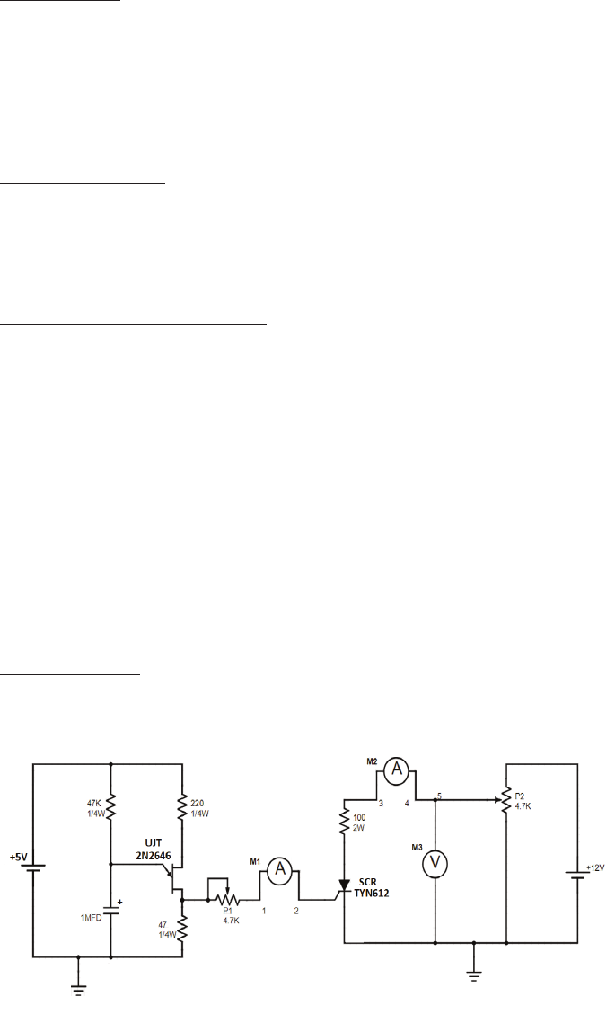
Experiment 16:
Triggering an SCR with a UJT
Introduction:
The triggering of an SCR using a UJT is a great way to demonstrate how a UJT operates as an oscillator. The
left side of the circuit is the UJT relaxation oscillator circuit setup. This will cause the UJT to continuously trigger
on and off, sending pulses to the SCR gate. This will then cause the SCR to trigger on and off, based on the
characteristics of the UJT. This, more advanced, circuit can be used to control motor speeds. While there are
more simple methods to control motors, this circuit combines knowledge from previous labs and expands on the
capabilities of the SCR.
Pre-Lab Questions:
In this circuit, which of the components produces the pulse to the emitter of the UJT?
How and when does this component create this pulse?
How does this process ultimately trigger the SCR?
Apparatus Required: Quantity
Resistance 47KΩ, ¼ W (on board) 1
Resistance 47Ω, ¼ W 1
Resistance 100Ω, 2W (on board) 1
Resistance 220Ω, ¼ W (on board) 1
Potentiometer 4.7KΩ (on board) 2
Ele. Cap 1MFD (on board) 1
UJT 2N2646 (on board) 1
SCR TYN 612 (on board) 1
Multimeter 3
Patch Cord 16
Circuit Diagram:
The circuit diagram for Triggering of SCR using UJT is shown below.
Figure 16

globalspecialties.com
Power Electronics Student Lab Manual
Procedure:
1. Connect the circuit, as shown in Figure 16, using patch cords.
2. Connect Ammeter between points ‘3’ and ‘4’ to measure Anode-cathode current IAK (mA).
3. Connect Ammeter between points ‘1’ and ‘2’ to measure the gate current Ig (mA).
4. Connect voltmeter at point ‘5’ and ground to measure the anode-cathode voltage Vak.
5. Rotate potentiometer P1 in the full clockwise position and P2 in the full counterclockwise position.
6. Switch Power ON.
7. Vary potentiometer P2 to increase the anode to cathode voltage. Set this voltage above 11V.
8. Vary potentiometer P1 to increase the value of gate current in steps. Record the measured current IAK
values on the table provided.
9. Initially there will be no current ow across the SCR. While increasing the gate current, the measured IAK
value will have a sudden jump and the measured VAK will have a sudden drop. This is an indication that the
SCR has been triggered.
10. After the ring on of the SCR, vary P1. There will be no effect on IAK or VAK.
11. To repeat this experiment, switch power OFF then follow the above Procedure from step 7.
Table 16: Measured Values
VAK
(V)
Gate Current
Anode to Cathode
Current
Anode to Cathode
Voltage
IAK
(mA)
No.
1
IG
(mA)
2
3
4
5
6
7
8
9
10

Power Electronics Student Lab Manual
44
Experiment 17:
Triggering an SCR with a IC-555
Introduction:
The 555 timer is an integrated circuit that can be used for such things as pulse generation and oscillator
applications. In this circuit, the 555 timer will act as an oscillator. The frequency of the 555 timer can be controlled
by adjusting the values of the two resistors and capacitor depicted on the left side of the circuit.
Pre-Lab Questions:
The 555 pinout diagram contains 8 pins. What is the function of each pin?
Apparatus Required: Quantity
Resistance 1KΩ, ¼ W 1
Resistance 100Ω, 2W (on board) 1
Resistance 5.1KΩ, ¼ W 1
IC 555 timer 1
Capacitor 0.01 MFD (on board) 1
Ele. Cap 1MFD (on board) 1
Diode IN4007 (on board) 1
SCR TYN 612 (on board) 1
Potentiometer 4.7KΩ (on board) 2
Multimeter 3
Patch Cord 17
Circuit Diagram:
The circuit diagram for Triggering of SCR using 555 IC is shown below:
Figure 17

globalspecialties.com
Power Electronics Student Lab Manual
Procedure:
1. Connect the circuit, as shown in Figure 17, using patch cords.
2. Connect ammeter between points ‘3’ and ‘4’ to measure Anode-cathode current IAK (mA).
3. Connect a second ammeter between points ‘1’ and ‘2’ to measure the gate Current IG (mA).
4. Connect voltmeter at point ‘5’ and ground to measure the anode–cathode voltage VAK.
5. Rotate potentiometer P1 in the full clockwise position and P2 in the full counterclockwise position.
6. Switch Power ON.
7. Vary potentiometer P2 to increase VAK. Set this voltage above 11V.
8. Vary potentiometer P1 to increase the value of gate current in steps. Record the measured IG values and
corresponding IAK measured values on the table provided.
9. Initially, there will be no current ow across the SCR. While increasing the gate current IG, there will be
a sudden increase in the measured IAK value and a sudden drop in the measured VAK value. This is an
indication that the SCR has been triggered.
10. Now vary the P1, there will be no effect on VAK or IAK.
11. To repeat this experiment switch power OFF and follow the Procedures starting from step 7.
Table 17: Measured Values
VAK
(V)
Gate Current
Anode to Cathode
Current
Anode to Cathode
Voltage
IAK
(mA)
No.
1
IG
(mA)
2
3
4
5
6
7
8
9
10
Power Electronics Student Lab Manual
46
Experiment 18:
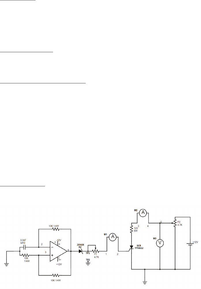
Triggering an SCR with a IC-741
Introduction:
An op amp is a device that converts a small signal input into a higher output. In this circuit the op amp is
congured as a mutivibrator circuit. The op amp will create a PWM signal to go through the Zener diode and
become the input of the SCR gate. This is an advanced circuit design that demonstrates one of the many ways to
trigger an SCR. Because it is advanced and impractical, this circuit is not used in typical electronic applications. In
this lab, the focus will be on the voltage across the SCR, to see when the op amp turns it off and on.
Pre-Lab Questions:
An Op Amp contains an inverting and noninverting terminal. Which pin, on the IC 741, is the inverting input and
which is the noninverting input?
Apparatus Required: Quantity
Resistance 10KΩ, ¼ W (on board) 3
Resistance 120Ω, 5W (on board) 1
Zener 9V (on board) 1
SCR TYN 612 (on board) 1
Potentiometer 4.7KΩ (on board) 2
IC 1M 741 1
Cap 0.047 MFD (on board) 1
Multimeter 3
Patch Cord 16
Circuit Diagram:
The circuit diagram for Triggering an SCR using IC -741 is shown below.
Figure 18

globalspecialties.com
Power Electronics Student Lab Manual
Procedure:
1. Connect the circuit, as shown in Figure 18, using patch cords.
2. Connect ammeter between points ‘3’ and ‘4’ to measure anode-cathode current IAK (mA).
3. Connect ammeter between points ‘1’ and ‘2’ to measure the gate Current IG (mA).
4. Connect voltmeter at point ‘5’ and ground to measure the anode-cathode voltage VAK.
5. Rotate the potentiometer P1 in the full clockwise position and P2 in the full counterclockwise position.
6. Switch Power ON.
7. Vary potentiometer P2 to increase VAK. Set this voltage above 11V.
8. Vary potentiometer P1 to increase the gate current IG value in steps. Record the measured VAK and
corresponding IAK values on the table provided.
9. Initially there will be no current ow across the SCR. While increasing the gate current IG, there will be
a sudden increase in the IAK measured value and a sudden drop in the VAK measured value. This is an
indication that the SCR has been triggered.
10. After the ring on of the SCR, vary the P1. There will be no effect on IAK or VAK.
11. To repeat this experiment switch power OFF and follow the Procedures starting from step 5.
Table 18: Measured Values
VAK (V)
Gate Current
Anode to Cathode
Current
Anode to Cathode
Voltage
IAK (mA)
No.
1
IG (mA)
2
3
4
5
6
7
8
9
10

Power Electronics Student Lab Manual
48
Experiment 19:
RAMP and Pedestal Triggering Using Anti parallel SCR
Introduction:
The ramp and pedestal triggering circuit is used to turn on and off two SCRs, connected in antiparallel, to power
an AC load. The potentiometer controls the pedestal voltage value and acts as the input voltage of the UJT.
When the UJT starts to conduct, a pulse is produced at the primary and secondaries of the transformer supplying
a pulse to the gate of the SCRs. In this lab the output across the load will be measured with an oscilloscope at
different ring angles of the two SCRs. The output should look like a sawtooth wave or a ramp as the title of the
circuit implies.
Pre-Lab Questions:
Through analysis of the circuit schematic for this lab, explain how potentiometer P1 controls the ring angle?
Apparatus Required: Quantity
Resistance 220Ω, 2W (on board) 1
Resistance 22KΩ, ¼ W (on board) 1
Resistance 220Ω, ¼ W 1
Resistance 1KΩ, 5W (on board) 1
Ele. Cap 1MFD (on board) 1
Diode IN4007 (on board) 8
Zener 9V (on board) 1
Potentiometer 4.7KΩ (on board) 1
UJT 2N2646 (on board) 1
SCR 2P4M (on board) 2
Pulse transformer 1:1:1 (on board) 1
Inductance 68mH (on board) 1
Patch cord 16

globalspecialties.com
Power Electronics Student Lab Manual
Circuit Diagram:
The circuit diagram of basic anti-parallel SCR in AC load is shown in the below Fig.19
Figure 19
Procedure:
1. Connect the circuit, as shown in Figure 19, using patch cords.
2. Rotate potentiometer P1 in the full clockwise position.
3. Switch Power ON.
4. Connect the oscilloscope and observe the output waveform across the load resistor and connect the
voltmeter across the load resistor.
5. Set the ring angle at 30°, 60°, 90°, 120°, and 150° by varying P1 and note the reading of output voltage.
Angle in time convert using T = (α x 10ms) / 180.
6. Observe the output waveform across load and across SCRs when ring angle is set to 90°.
Table 19: Observed Values
Output Voltage
(V
rms
)
Output Across AC Load Circuit
No.
Input AC Voltage
(V
rms)
Firing Angle
(Degrees)
1
2
3
4
5
6
7
8
9
10

Power Electronics Student Lab Manual
50
Image 19: Ramp and Pedestal Circuit Waveform

globalspecialties.com
Power Electronics Student Lab Manual
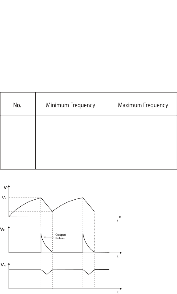
Experiment 20:
UJT Relaxation Oscillator
Introduction:
The UJT component is commonly used in the UJT Relaxation Oscillator circuit. The relaxation oscillator is
controlled by the charging and discharging of a capacitor. This causes the oscillation of the circuit and allows the
UJT to be used in many different applications. Paired with an SCR, the UJT can be used to apply a pulse to the
gate of an SCR making a triggering circuit with the two power components. The oscillation time is in the range of
nanoseconds making it a fast and efcient switching device.
Pre-Lab Questions:
For the circuit in this lab, will the capacitor charge and discharge at the same rate? Why?
When will the capacitor trigger the UJT?
Apparatus Required: Quantity
Resistance 10KΩ, ¼ W (on board) 1
Resistance 220Ω, ¼ W 1
Resistance 100Ω, ¼ W (on board) 1
Diode IN4007 (on board) 1
Cap. 0.1MFD (on board) 1
UJT 2N2646 (on board) 1
Potentiometer 4.7KΩ (on board) 1
Patch cord 10
Circuit Diagram:
The UJT Relaxation Oscillator circuit diagram is shown below:
Figure 20
Power Electronics Student Lab Manual
52
Procedure:
1. Connect the circuit, as shown in Figure 20, using patch cords.
2. Rotate potentiometer P1 in the full clockwise position.
3. Switch Power ON.
4. Connect the oscilloscope CH1 between output and ground and CHII between TP1 and ground, observe the
waveform of pulse output and RC time constant.
5. Vary potentiometer P1 to increase the frequency of the output.
6. Connect the oscilloscope CH1 between output and ground and CHII between TP1 and ground, observe the
waveform of pulse output and RC time constant.
7. Vary potentiometer P1 to increase the frequency of the output.
Table 20: Observed Values
Image 20: UJT Relaxation Oscillator Waveform

globalspecialties.com
Power Electronics Student Lab Manual
Experiment 21:
Voltage Commutated Chopper
Introduction:
The Voltage Commutated Chopper circuit is used to control the power consumed at the load. The circuit does this by
chopping the source voltage waveform to a lower value. It was commonly used in dimmer switches and incandescent
lamps to control power output. The advantage of this circuit is the components, used in it, are inexpensive. The
disadvantage of this circuit is the harmonics created inside the circuit as well as its limitations when working with
inductive loads.
Pre-Lab Questions:
The Voltage Commutated Chopper can be broken up into 4 modes. What occurs at each of these modes when
the circuit is on?
Apparatus Required: Quantity
Resistance 510Ω, ¼ W 1
Met. Cap. 0.33MFD (on board) 1
Inductor 68mH (on board) 1
Inductor 10mH (on board) 1
SCR 2P4M (on board) 2
Diode IN4007 (on board) 2
Patch cord 10
Circuit Diagram:
Circuit diagram of voltage commutated chopper is shown below:
Figure 21
Procedure:

Power Electronics Student Lab Manual
54
1. Connect the circuit as shown in Figure 21
2. Connect G1 & G2 to the gate of SCR1 and SCR2.
3. Switch ON the LAB.
4. Vary the PWM Pot in fully clockwise direction.
5. Connect the oscilloscope across the load.
6. Vary the frequency potentiometer and observe the output across load, SCR1, and SCR2.
Table 21: Observed Values
Output Voltage
Frequency
No.
1
2
3
4
5
6
7
8
9
10
Image 21: Voltage Commutated Chopper Waveform

globalspecialties.com
Power Electronics Student Lab Manual
Experiment 22:
Bedford Inverter
Introduction:
Inverters are typical Power Electronics circuits that take in a DC voltage and convert it to an AC voltage.
This is helpful when transmitting voltages across components that are DC sensitive. The Bedford inverter is a full
bridge converter that converts DC voltage into AC voltage. It uses SCRs to form two separate half bridge circuits
when connected from a full AC voltage wave. This is a very powerful converter, and many variations of this circuit
are used in common electronic appliances.
Apparatus Required: Quantity
Resistance 33KΩ, ¼ W (on board) 1
Met. Cap 1MFD 63V (on board) 4
SCR 2P4M (on board) 4
Diode IN4007 (on board) 4
Patch cord 10
Circuit diagram:
Circuit diagram of Bedford inverter is shown below:
Figure 22

Power Electronics Student Lab Manual
56
Procedure:
1. Connect the circuit as shown in Figure 22
2. Connect G1, G2, G3, and G4 to the gate of SCR1, SCR2, SCR3, and SCR4 respectively.
3. Switch Power ON.
4. Rotate the PWM and Frequency CONTROL to set between the full counterclockwise and midpoint position.
5. Connect oscilloscope across the load and SCR’S.
6. Vary FREQUENCY pot and observe the output across load and across SCR1 & SCR2
Table 22: Observed Values
Output Voltage
Frequency
No.
1
2
3
4
5
6
7
8
9
10

globalspecialties.com
Power Electronics Student Lab Manual
Experiment 23:
Single Phase PWM Inverter with MOSFET
Introduction:
While utilizing an SCR is a common way to create an inverter, the same can be achieved with MOSFETS.
The single phase PWM inverter uses MOSFETS to control the fast switching of the voltage across the load.
Connecting a DC input and switch to this MOSFET circuit formation inverts the signal into an AC output. When
G1 and G3 are conducting there is a positive voltage drop across the resistor. When G2 and G4 are conducting
there is negative voltage across the resistor. This along with the current direction change results in a DC to AC
conversion.
Pre-Lab Questions:
In this circuit, how is DC converted to AC?
Why is the ring sequence of G1, G2, G3, and G4 important for the circuit to operate effectively?
Apparatus Required: Quantity
MOSFET IRF540 (on board) 1
MOSFET IRF 540 3
Resistance 1KΩ, 1/5 W (on board) 1
Switch 1P-2W (SPOT) on board 1
Patch cord 10
Circuit Diagram:
Circuit diagram of a Single Phase PWM Inverter is shown below:
Figure 23

Power Electronics Student Lab Manual
58
Procedure:
1. Connect the circuit as shown in Figure 23
2. Rotate the FREQUENCY pot. in the full counterclockwise position and the PWM CONTROL in the full
clockwise position.
3. Switch Power ON.
4. Vary FREQUENCY pot. and observe waveform across load on oscilloscope.
5. Set the maximum frequency.
6. Connect the voltmeter across the load and measure the AC voltage.
7. Vary PWM CONTROL and observe output waveform across load and note the readings of pulse width and
corresponding output AC (rms) voltage across load.
Table 23: Observed Values
Image 23: PWM Inverter Waveform

globalspecialties.com
Power Electronics Student Lab Manual
Experiment 24:
Single Phase PWM Inverter with IGBT
Introduction:
The single phase PWM inverter using IGBTs is very similar to the MOSFET equivalent in experiment 23. The
IGBTs are triggered in the same fashion as the MOSFETs, with a signal applied to the gate. The DC input voltage
is regulated using a control switch. The two circuits produce the same result and mirror each other in circuit
design and complexity. This lab will demonstrate how the PWM Inverter circuit produces the same results when
using either IGBTs or MOSFETs
Pre-Lab Questions:
In this circuit, how is DC converted to AC?
Why is the ring sequence of G1, G2, G3, and G4 important for the circuit to operate effectively?
Apparatus Required: Quantity
IGBT G4BC20S (on board) 1
IGBT G4BC20S 3
Resistance 1KΩ 5W (on board) 1
Tiny Toggle switch SPDT (on board) 1
Patch cord 10
Circuit Diagram:
Circuit diagram of a Single Phase PWM Inverter is shown below:
Figure 24

Power Electronics Student Lab Manual
60
Procedure:
1. Connect the circuit as shown in Figure 24.
2. Rotate the FREQUENCY pot. in the full counterclockwise position and PWM CONTROL in the full clockwise
position.
3. Switch Power ON.
4. Vary the FREQUENCY pot. and observe waveform across load on oscilloscope.
5. Set the maximum frequency.
6. Connect the voltmeter across the load and measure the AC voltage.
7. Vary PWM CONTROL and observe output waveform across load and note the readings of pulse width and
corresponding output AC (rms) voltage across load.
Table 24: Observed Values
Image 24: PWM Inverter Waveform

globalspecialties.com
Power Electronics Student Lab Manual
Experiment 25:
Half Wave Controlled Rectier with Resistive Load
Introduction:
The half wave rectier circuit converts an AC source into DC voltage for a load. The SCR can be triggered at
different ring angles. This can only be done during the positive cycle of the AC voltage, making it a half wave
circuit. This circuit is used in many basic dimmer switch applications but is usually replaced by the full wave
version of it. In this lab the ring angle will be varied to see the change in output voltage, using an oscilloscope.
The oscilloscope will show how output voltage is only present during the positive AC source voltage cycle.
Pre-Lab Questions:
Why does the V vs ωt graph, for this circuit, equal 0 between π and 2π?
How is the ring angle α being controlled in this circuit?
Apparatus Required: Quantity
SCR 2P4M (on board) 1
Resistance 1KΩ, 5W (on board) 1
Multimeter 2
Patch cord 5
Circuit Diagram:
The circuit diagram of a basic Half-wave Controlled Rectier is shown below.
Figure 25

Power Electronics Student Lab Manual
62
Procedure:
1. Connect the circuit as shown in Figure 25.
2. Rotate “FIRING ANGLE CONTROL POT” in the full clockwise position.
3. Switch Power ON.
4. Measure the AC voltage (Vrms) by voltmeter between point 0V-15V and calculate Em by Em = 1.414 X
Vrms.
5. Switch Power OFF.
6. Connect circuit as shown in Figure 25.
7. Switch Power ON.
8. Connect the oscilloscope across the Load.
9. Connect the ammeter between Load and SCR.
10. Vary the ring control pot and set on 30°, 60°, 90°, 120° and 150° ring angles using T = (a X 10ms) / 180.
11. Observe the output waveforms and note the readings of voltage across Load at different ring angles.
12. Observe the waveform across the SCR1 when ring angle is 90°.
13. Calculate the average load Idc current and power Pdc from measured load voltage Vo.
Table 25: Observed Values
Calculated
(Vdc)
Measured
(V
0
)
Calculated
(P
dc
) I
dc
x
V
dc
Measured
(P
0
) I
0
x V
0
Calculated
(I
dc
)
V
dc
/R
L
Measured
(I
0
) V
0
/R
L
Input AC Voltage
Firing Angle
Average Output
Voltage Across Load
Average Load Current
Average Output
Power
7
8
9
No.
V
rms
V
M
Degrees
Time
(ms)
10
1
2
3
4
5
6
Image 25: Half Wave Rectier with Resistive Load Circuit Waveform

globalspecialties.com
Power Electronics Student Lab Manual
Experiment 26:
Half Wave Controlled Rectier with RL Load
Introduction:
The half wave rectier circuit with an RL load is similar to the purely resistive load circuit. The added inductor
makes it a more realistic circuit, as loads usually have both resistance and inductance. The circuit is still a half
wave rectier, so it only conducts during the positive cycle of the AC source. The output will continue to conduct
after the SCR has been turned off due to the inductor at the load resulting in a different output voltage. This lab
will focus on the output voltage waveform to see how it differs from the previous lab.
Pre-Lab Questions:
1) Why does the V vs ωt graph, for this circuit, equal 0 between π and 2π?
2) How is the ring angle α being controlled in this circuit?
3) How will adding an inductor to the resistive load affect the V vs ωt graph?
Apparatus Required: Quantity
SCR 2P4M (on board) 1
Resistance 270Ω / 5W (on board) 1
Inductor 68mH (on board) 2
Multimeter 2
Patch cord 7
Circuit Diagram:
The circuit diagram for a basic Half-Wave Controlled Rectier is shown below.
Figure 26

Power Electronics Student Lab Manual
64
Procedure:
1. Connect the circuit as shown in Figure 26.
2. Rotate “FIRING ANGLE CONTROL POT” in the full clockwise position.
3. Switch Power ON.
4. Measure the AC voltage (Vrms) by voltmeter between points 0V-15V. Calculate Em. Em = 1.414 X Vrms.
5. Switch Power OFF.
6. Connect the circuit as shown in Figure 26.
7. Switch Power ON.
8. Connect the oscilloscope across load.
9. Connect the ammeter between Load and SCR.
10. Vary the “FIRING ANGLE CONTROL POT” and set to 30°, 60°, 90°, 120° and 150° ring angles using T =
(α X 10ms) / 180.
11. Observe the output waveforms and note the readings of voltage across load at different ring angles.
12. Observe the waveform across the SCR1 when ring angle is 90°.
13. Calculate the average load Idc current and power P dc from measured load voltage Vo.
Table 26: Observed Values
Calculated
(Vdc)
Measured
(V
0
)
Calculated
(P
dc
) I
dc
x
V
dc
Measured
(P
0
) I
0
x V
0
Calculated
(I
dc
)
V
dc
/R
L
Measured
(I
0
) V
0
/R
L
Input AC Voltage
Firing Angle
Average Output
Voltage Across Load
Average Load Current
Average Output
Power
7
8
9
No.
V
rms
V
M
Degrees
Time
(ms)
10
1
2
3
4
5
6
Image 26: Half Wave Rectier with Resistive- Inductive Load Circuit Waveform

globalspecialties.com
Power Electronics Student Lab Manual
Experiment 27:
Full-Wave Controlled Rectier (Mid Point Conguration)
with Resistive Load
Introduction:
The full bridge rectier, midpoint conguration, is a continuation of the half wave rectier. This circuit contains an
additional SCR. Both SCRs are connected to an AC source. During the positive cycle of the source voltage, the
rst SCR is triggered based on the ring angle while the second SCR is triggered during the negative cycle. This
circuit utilizes the entire AC voltage source wave, making it more efcient. In this lab the ring angle will be varied
to view, on an oscilloscope, the change in the output voltage.
Pre-Lab Questions:
If the power source for this lab is AC, why isn’t the voltage across the load ever negative?
Apparatus Required: Quantity
SCR 2P4M (on board) 2
Resistance 1KΩ, 5W (on board) 1
Multimeter 2
Patch cord 9
Circuit Diagram:
The circuit diagram for a basic Full-Wave Controlled Rectier (Mid-Point conguration) is shown below.
Figure 27

Power Electronics Student Lab Manual
66
Procedure:
1. Connect the circuit as shown in Figure 27.
2. Rotate “FIRING ANGLE CONTROL POT” in the clockwise position.
3. Switch Power ON.
4. Measure the ac voltage (Vrms) by voltmeter between points 0V-15V. Calculate Em. Em = 1.414 X Vrms.
5. Switch Power OFF.
6. Connect circuit, as shown in Figure 27, using patch cords.
7. Switch Power ON.
8. Connect the oscilloscope across the Load.
9. Connect the ammeter between Load and SCR, as shown in circuit diagram.
10. Vary “FIRING ANGLE CONTROL POT” and set to 30°, 60°, 90°, 120° and 150° ring angles using T = (α X
10ms) / 180.
11. Observe the output waveforms and note the readings of voltage across Load at different ring angle.
12. Connect oscilloscope across SCR1 only and observe the waveform when ring angle is 90°.
13. Connect oscilloscope across SCR2 only and observe the waveform when ring angle is 90°.
14. Calculate the average Load Idc current and power Pdc from measured load voltage Vo.
Table 27: Observed Values
Calculated
(Vdc)
Measured
(V
0
)
Calculated
(P
dc
) I
dc
x
V
dc
Measured
(P
0
) I
0
x V
0
Calculated
(I
dc
)
V
dc
/R
L
Measured
(I
0
) V
0
/R
L
Input AC Voltage
Firing Angle
Average Output
Voltage Across Load
Average Load Current
Average Output
Power
7
8
9
No.
V
rms
V
M
Degrees
Time
(ms)
10
1
2
3
4
5
6

globalspecialties.com
Power Electronics Student Lab Manual
Image 27: Full Wave Rectier (Mid-Point) with Resistive Load Circuit Waveform

Power Electronics Student Lab Manual
68
Experiment 28:
Full-Wave Controlled Rectier (Mid Point Conguration)
with RL Load
Introduction:
The full bridge rectier, midpoint conguration, with an RL load is similar to the circuit with only a resistive load.
The inductor continues to store charge after the SCR has been turned off causing the output waveform to produce
a negative voltage. This is common in many electronic load circuits. In this lab the ring angle will be varied to
view, on an oscilloscope, the change in the output voltage.
Pre-Lab Questions:
How will the inductor, added to this circuit, affect the voltage across the load?
Apparatus Required: Quantity
SCR 2P4M (on board) 2
Resistance 270Ω/5W (on board) 1
Inductors 68mH (on board) 2
Multimeter 2
Patch Cord 11
Circuit Diagram:
The circuit diagram for a basic Full–Wave Controlled Rectier (Mid-Point conguration) is shown below.
Figure 28

globalspecialties.com
Power Electronics Student Lab Manual
Procedure:
1. Connect the circuit as shown in Figure 28.
2. Rotate “FIRING ANGLE CONTROL POT” in the full clockwise position.
3. Switch Power ON.
4. Measure the AC voltage (Vrms) by connecting the voltmeter between points 0V-15V and calculate Em by
Em = 1.414 X Vrms.
5. Switch Power OFF.
6. Connect circuit as shown in Figure 28.
7. Switch Power ON.
8. Connect the oscilloscope across the Load.
9. Connect the ammeter between Load and SCR, as shown in circuit diagram.
10. Vary “FIRING ANGLE CONTROL POT” and set to 30°, 60°, 90°, 120° and 150° ring angles using T = (α X
10ms) / 180.
11. Observe the output waveforms and note the readings of voltage across Load at different ring angle.
12. Connect oscilloscope across SCR1 only and observe the waveform when ring angle is 90°.
13. Connect oscilloscope across SCR2 only and observe the waveform when ring angle is 90°.
14. Calculate the averageLoad Idc current and power Pdc from measured Load voltage Vo.
Table 28: Observed Values
Calculated
(Vdc)
Measured
(V
0
)
Calculated
(P
dc
) I
dc
x
V
dc
Measured
(P
0
) I
0
x V
0
Calculated
(I
dc
)
V
dc
/R
L
Measured
(I
0
) V
0
/R
L
Input AC Voltage
Firing Angle
Average Output
Voltage Across Load
Average Load Current
Average Output
Power
7
8
9
No.
V
rms
V
M
Degrees
Time
(ms)
10
1
2
3
4
5
6
Image 28: Full Wave Rectier (Mid-Point) with Resistive-Inductive Load Circuit Waveform

Power Electronics Student Lab Manual
70
Experiment 29:
Fully Controlled Bridge Rectier with Resistive Load
Introduction:
The fully controlled bridge rectier circuit takes an AC source and converts it into a DC voltage output load. It is
a full bridge rectier because it supplies power across the entire AC wave. A normal full bridge rectier, using
diodes, supplies the signal after the diode voltage is met. Using SCRs, the ring angle can be adjusted to trigger
the output supply to the load voltage at a specic point on the AC wave. In this lab the ring angle will be varied to
view, on an oscilloscope, the change in the output voltage.
Pre-Lab Questions:
In this lab AC will be converted to DC, using four thyristors as labeled on the circuit diagram provided. To achieve
this, two thyristors must be red on simultaneously as pairs. What should be the thyristor ring sequence for the
circuit to operate correctly?
Apparatus Required: Quantity
SCR 2P4M (on board) 4
Resistance 1KΩ, 5W (on board) 1
Multimeter 2
Patch Cord 16
Circuit Diagram:
The circuit diagram for a basic Fully Controlled Bridge Rectier is shown below.
Figure 29

globalspecialties.com
Power Electronics Student Lab Manual
Procedure:
1. Connect the circuit as shown in Figure 29.
2. Rotate “FIRING ANGLE CONTROL POT” in the full clockwise position.
3. Switch Power ON.
4. Measure the AC voltage (Vrms) by connecting voltmeter between points 0V-15V and calculate Em by Em =
1.414 X Vrms.
5. Switch Power OFF.
6. Connect circuit as shown in Figure 29.
7. Switch Power ON.
8. Connect the oscilloscope across the Load.
9. Connect the ammeter between SCR and Load, as shown in Figure 29.
10. Vary “FIRING ANGLE CONTROL POT” and set to 30°, 60°, 90°, 120° and 150° ring angles using T = (α X
10ms) / 180.
11. Observe the output waveforms and note the readings of voltage across Load at different ring angle.
12. Connect the oscilloscope one by one across SCR1, SCR2, SCR3, and SCR4, observe the waveforms for
each when ring angle is 90°.
13. Calculate the average Load Idc current and power Pdc from measured load voltage Vo.
Table 29: Observed Values
Calculated
(Vdc)
Measured
(V
0
)
Calculated
(P
dc
) I
dc
x
V
dc
Measured
(P
0
) I
0
x V
0
Calculated
(I
dc
)
V
dc
/R
L
Measured
(I
0
) V
0
/R
L
Input AC Voltage
Firing Angle
Average Output
Voltage Across Load
Average Load Current
Average Output
Power
7
8
9
No.
V
rms
V
M
Degrees
Time
(ms)
10
1
2
3
4
5
6
Image 29: Full Wave Bridge Rectier with Resistive Load Circuit Waveform

Power Electronics Student Lab Manual
72
Experiment 30:
Fully Controlled Bridge Rectier with RL Load
Introduction:
The fully controlled bridge rectier circuit with an RL load is like the previous circuit with a varying output. The
full bridge circuit with only a resistor at the load will have time periods where the voltage output is zero. With the
addition of an inductor, to the load, the output voltage becomes continuous as the inductor supplies additional
power during the time period where the SCR has not been triggered. This helps create a more realistic output
curve as many common loads have both a resistive and inductive portion. In this lab the ring angle will be varied
to see the change in the output voltage on an oscilloscope.
Pre-Lab Questions:
1. In this lab AC will be converted to DC, using four thyristors as labeled on the circuit diagram provided. To
achieve this, two thyristors must be red on simultaneously as pairs. What should be the thyristor ring
sequence for the circuit to operate correctly?
2. How will the inductor, added in this circuit, affect the voltage across the load?
Apparatus Required: Quantity
SCR 2P4M (on board) 4
Resistance 270Ω, 5W (on board) 1
Inductor 68mH (on board) 2
Multimeter 2
Patch Cord 10
Circuit Diagram:
The circuit diagram for a basic Fully Controlled Bridge Rectier is shown below.
Figure 30
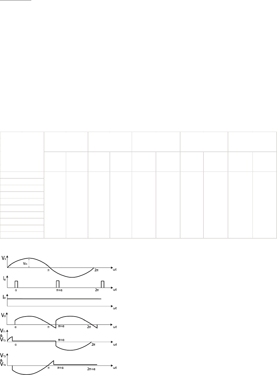
globalspecialties.com
Power Electronics Student Lab Manual
Procedure:
1. Connect the circuit as shown in Figure 30.
2. Rotate “FIRING ANGLE CONTROL POT” in the full clockwise position.
3. Switch Power ON.
4. Measure the AC voltage (Vrms) by connecting voltmeter between points 0V-15V and calculate Em by Em =
1.414 X Vrms.
5. Switch Power OFF.
6. Connect circuit, as shown in Figure 30, using patch cords.
7. Switch Power ON.
8. Connect the oscilloscope across the Load.
9. Connect the ammeter between SCR and Load, as shown in Figure 30.
10. Vary “FIRING ANGLE CONTROL POT” and set to 30°, 60°, 90°, 120° and 150° ring angles using T = (α X
10ms) / 180.
11. Observe the output waveforms and note the readings of voltage across Load at different ring angles.
12. Connect the oscilloscope one by one across SCR1, SCR2, SCR3, and SCR4, observe the waveforms for
each when ring angle is 90°.
13. Calculate the average Load Idc current and power Pdc from measured load voltage Vo.
Table 30: Observed Values
Calculated
(Vdc)
Measured
(V0)
Calculated
(Pdc) Idc
x
Vdc
Measured
(P
0) I
0 x V0
Calculated
(Idc)
Vdc/RL
Measured
(I0) V0/RL
Input AC Voltage
Firing Angle
Average Output
Voltage Across Load
Average Load Current
Average Output
Power
7
8
9
No.
Vrms
VM
Degrees
Time
(ms)
10
1
2
3
4
5
6
Image 30: Full Wave Bridge Rectier with Resistive- Inductive Load Circuit Waveform

Power Electronics Student Lab Manual
74
Experiment 31:
Low Side Buck Converter with Resistive Load
Introduction:
The buck converter with a resistive load is a very common and critically important circuit in many electrical circuit
designs. The purpose of the buck converter is to take a DC input supplied at a certain voltage and “buck” it
down to a different voltage level. The reason a buck converter is used over a simple voltage divided is due to the
efciency. Buck converters maintain an overall efciency of 90% or higher while voltage dividers can lose up to
half the energy to the resistor in the divider circuit. The buck converter is used in cell phones, LED applications,
almost anywhere where multiple circuit components are being powered but at different voltage levels. In this lab
the duty cycle will be changed to show how the output voltage is affected by this.
Pre-Lab Questions:
What feature of this circuit enables it to step down the voltage?
Apparatus Required: Quantity
Patch Cords 9
MOSFET Switch (on board) 1
Resistance 120, 5W (on board) 1
Inductance 250µH 1
Capacitance 100µF 1
Diode IN4007 (on board) 1
Function Generator 1
Circuit Diagram:
The circuit diagram of the low side buck converter is shown in the below.
Figure 31

globalspecialties.com
Power Electronics Student Lab Manual
Procedure:
1. Make connections according to Fig.31
2. The function generator (FG) has the positive lead (A1) connected to the MOSFET gate G
3. The negative lead (A2) of the function generator is connected to ground
4. The inductor (L1) and capacitor (C1) components are found in the kit and should be placed onto the bread
board for this lab section.
5. Set the function generator to a 5V, 100 kHz square wave with a 2.5V offset
6. Set the duty cycle to an initial value of 50%
7. Switch ON the power
8. Connect the voltmeter across the load
9. Vary the duty cycle from 20%, 25%, 30%, 35%, 40%, 45%, 50%, 55%, 60%, 65%, 70%, 75% on the
function generator
10. Observe the readings of the voltage across the load at different duty cycles
11. Create a graph of Vo/Vin vs Duty Cycle. Is there a trend?
Table 31: Observed Values:
70%
60%
55%
50%
75%
45%
40%
35%
30%
Duty Cycle
Vo
Vo / Vin
20%
25%
Image 31: Low Side Buck Converter with Resistive Load

Power Electronics Student Lab Manual
76
Experiment 32:
Boost Converter with Resistive Load
Introduction:
The Boost Converter circuit can be referred to as a power converter. It will step up voltage, resulting in an output
voltage greater than the input. Because power is directly proportional to voltage, this circuit is sometimes referred
to as a power converter. It operates with a suitable DC power source, such as a battery. This makes it ideal for
battery power systems where space is limited. Hybrid Vehicles utilize this type of system. Rather than stacking
battery cells to increase power, a boost converter may be employed to increase power. The benets of a boost
converter circuit are easily recognizable in these type of circuits.
Pre-Lab Questions:
1) What feature of this circuit enables it to produce a higher output than input voltage?
Apparatus Required: Quantity
Patch Cords 9
MOSFET Switch (on board) 1
Resistance 120/5W (on board) 1
Inductance 250µH 1
Capacitance 100µF 1
Diode (on board) 1
Function Generator 1
Circuit Diagram:
The circuit diagram of the boost converter is shown in the below.
Figure 32

globalspecialties.com
Power Electronics Student Lab Manual
Procedure:
1. Make connections according to Fig.32
2. The function generator (FG) has the positive lead (A1) connected to the MOSFET gate G
3. The negative lead (A2) of the function generator is connected to ground.
4. The inductor (L1) and capacitor (C1) components are found in the kit and should be placed onto the bread
board for this lab section.
5. Set the function generator to a 5V, 50 KHz square wave with a 2.5V offset
6. Set the duty cycle to an initial value of 50%
7. Switch ON the power
8. Connect the voltmeter across the load
9. Vary the duty cycle from 20%, 25%, 30%, 35%, 40%, 45%, 50%, 55%, 60%, 65%, 70%, 75% on the
function generator
10. Observe the readings of the voltage across the load at different duty cycles
11. Create a graph of Vo/Vin vs Duty Cycle. Is there a trend?
Table 32: Observed Values:
70%
60%
55%
50%
75%
45%
40%
35%
30%
Duty Cycle
Vo
Vo / Vin
20%
25%
Image 32: Boost Converter with Resistive Load

Power Electronics Student Lab Manual
78
Experiment 33:
Buck-Boost Converter with Resistive Load
Introduction:
The Buck-Boost Converter can perform the functions of both a Buck Converter and Boost Converter. Because
both circuits use similar components, the Buck-Boost Converter can be constructed by rearranging and
connecting these components accordingly. It can step down or step up the voltage of any compatible DC power
source connected to it.
Apparatus Required: Quantity
Patch Cords 9
MOSFET Switch (on board) 1
Resistance 120/5W (on board) 1
Inductance 250µH 1
Capacitance 100µF 1
Diode (on board) 1
Function Generator 1
Circuit diagram:
The circuit diagram of the buck-boost converter is shown in the below.
Figure 33

globalspecialties.com
Power Electronics Student Lab Manual
Procedure
1. Make connections according to Fig.33
2. The function generator (FG) has the positive lead (A1) connected to the MOSFET gate G.
3. The negative lead (A2) of the function generator is connected to ground
4. The inductor (L1) and capacitor (C1) components are found in the kit and should be placed onto the bread
board for this lab section.
5. Set the function generator to a 5V, 50 KHz square wave with a 2.5V offset
6. Set the duty cycle to an initial value of 50%
7. Switch ON the power
8. Connect the voltmeter across the load
9. Vary the duty cycle from 20%, 25%, 30%, 35%, 40%, 45%, 50%, 55%, 60%, 65%, 70%, 75% on the
function generator
10. Observe the readings of the voltage across the load at different duty cycles
11. Create a graph of Vo/Vin vs Duty Cycle. Is there a trend?
Table 33: Observed Values:
70%
60%
55%
50%
75%
45%
40%
35%
30%
Duty Cycle
Vo
Vo / Vin
20%
25%
Image 33: Buck-Boost Converter with Resistive Load

Power Electronics Student Lab Manual
80
Answers (Pre-Lab)
Lab 1
1. An SCR has three leads whereas a diode is a two lead component. In addition, the P-N structure of an SCR
contains three junctions, a diode only has one.
2.
3. Doping Is the process where impurities are added to the crystalline structure of the semiconductor
material. The impurities will either provide free electrons (donor) or holes (acceptor) to the material. N-type
semiconductors are doped with donor elements, and P-type semiconductors are doped with acceptor
elements.
Lab 2
1. With forward biased at the anode and cathode, the SCR can produce current with the gate open or with a
positive voltage applied to the gate.
2. Breakover voltage is the voltage at which the SCR begins producing forward current. With no gate current,
the breakover voltage is much higher.
3. The holding current is the minimum anode current required to keep the SCR operating. If the anode current
is less than the holding current, the SCR will shut off.
Lab 3
The UJT is made up of lightly doped N-Type material bar with a heavily doped P-typed strip of material attached
to the end, creating a P-N junction. Base 1 and Base 2 leads are in ohmic contact at the ends of the N-type
material, and the gate is connected to the P-type material.
Because the emitter is connected to the P-type material, P-N junction acts as a diode allowing the emitter current
to ow in only one direction. The emitter current induces in to the base region, and the resistance between emitter
junction and base 1 lowers.
The inter-base resistance is the resistance between base 1 and base 2, when the emitter acts as an open circuit.
The intrinsic stand-off ratio is the resistance between the emitter junction and base 1 as a ratio to the inter-base
resistance.
Lab 4
As the name implies, this type of transistor uses an electric eld effect to create channels. When a positive
voltage is applied to the gate, the positive charge will repel the positive charge carriers away from the P-type
substrate surface and form a narrow channel of negative charge carriers. The SCR and UJT do not depend on
electric eld effects for the makeup of their P-N junctions.
N-Channel
It consists of a P-type substrate with two sections of N-type material. The N-type sections are near the surface of
the bulk and separated. In the separated space is where the channel will form.
Lab 5
A higher gate current will result in a higher current ow through the device
600V
Lab 6
A DIAC is different from an ordinary diode in that it can conduct current ow in a bi-directional manner.
Two diodes in parallel and in opposite directions
32V

globalspecialties.com
Power Electronics Student Lab Manual
Lab 7
A TRIAC and a DIAC can both conduct current in a bidirectional fashion
A TRIAC is triggered by a gate. A DIAC does not contain a gate lead.
Lab 8
The peak voltage is the sum of the gate voltage and one diode drop. Vp = VG + .7
2.7V, 5.7V, 10.7V
Given the circuit connection, the resistors determine the voltage drop at VG. This directly affects VG which
determines the value of VP.
Lab 9
When the power is switched on, the SCR is off and the capacitor charges up with the polarity depicted on the
circuit. A pulse triggers the SCR, causing it to begin conducting. The capacitor will discharge and begin to
recharge with the reverse polarity. As a result, a commutating current, from the capacitor, will begin to ow in
opposite direction of the load current. When the commutating current becomes greater than the load current, the
SCR will shut off.
Lab 10
In this lab, if SCR1 is rst triggered, by a pulse to the gate, the capacitor will charge with a positive voltage on the
right and negative voltage on the left. When SCR2 is triggered, by a pulse to the gate, the negative polarity from
the capacitor will be applied to the anode of SCR1, and SCR1 will also have a positive polarity at the cathode.
This reverse bias, across SCR1, will effectively shut it off. SCR2 will shut off in the same manner, once SCR1 is
triggered again.
Lab 11
The same does not occur in the class D commutation circuit. IF SCR2 is red on rst the capacitor will begin to
charge. Once the capacitor is fully charged the negative polarity of it will be connected to the anode of SCR2. This
will decrease the current owing through SCR2 eventually shutting it off. In Class D commutation, SCR2 will shut
off without ever having to re on SCR1.
Lab 12
Once the SCR is triggered, it will remain on between 0 and π because the power source is alternating current. The
SCR will shut off and remain off between π and 2π because the SCR will be in reverse biased.
Lab 13
The potentiometer affects when the SCR res on because it can increase and decrease the gate current.
Breakover voltage is contingent on gate current.
Because the maximum applied voltage is at 90°, the minimum gate current, to trigger the SCR, is reached
between 0 and 90°.
Lab 14
Resistor triggering circuit can only re on the SCR between phase angle 0 to 90°. Resistor capacitor triggering
circuit has a ring angle range of 0 to 180°
Lab 15
The Resistance value determines the capacitor time constant. By varying the potentiometer, the capacitor
charging time increases or decreases. The faster the capacitor charges to the triggering gate voltage, the sooner
it will trigger the SCR.

Power Electronics Student Lab Manual
82
Lab 16
The capacitor
When the capacitor voltage reaches the peak value of the UJT, it begins to conduct. The conduction will continue
until the capacitor voltage is equal to the valley voltage of the UJT. This will be a repeating process, effectively
creating pulses.
Base 1 of the UJT is connected to the gate of the SCR. Because of this, the pulse output at base 1 will re on the
SCR.
Lab 17
Pin1 = Ground; Pin2 = Trigger; Pin3 = Output; Pin4 = Reset; Pin5 = Control; Pin6 = Threshold; Pin7 =
Discharge; Pin8 = Supply Voltage
Lab 18
Pin2 = inverting input; Pin3 = noninverting input
Lab 19
Adjusting the potentiometer will control the pedestal voltage. The pedestal voltage directly affects the charging
time of the capacitor to reach the threshold voltage of the UJT. When the capacitor charges to the threshold
voltage of the UJT, it triggers it sending a pulse to the SCR. The higher the pedestal voltage the sooner the
capacitor will charge to the threshold voltage, resulting in the ring angle being less. With a lower pedestal voltage
value, the capacitor will take longer to charge increasing the ring angle.
Lab 20
The capacitor will discharge more rapidly than it charges. This is due to the resistor connected at base 1 having
such low resistance.
Because the capacitor is connected to the emitter, the UJT is triggered when the capacitor voltage reaches the
diode volt drop value.
Lab 21
Mode 1 = T1 is red on and the capacitor begins to discharge and recharge with reverse polarity
Mode 2 = The capacitor is fully charged and T1 continues to conduct.
Mode 3 = T2 is triggered and the capacitor begins to discharge again. The voltage across T1 is negative, shutting
it off.
Mode 4 = The capacitor discharges and recharges with opposite polarity. The current through T2 decays shutting
it off.
Lab 23
DC is being converted into AC through the 1K Load only. This is achieved by simultaneously triggering two
MOSFET at a time.
It is important G1 and G3 be triggered simultaneously while G2 and G4 remain off, and vice versa. This will strictly
control the current through the load in an alternating manner.
Lab 24
DC is being converted into AC through the 1K Load only. This is achieved by simultaneously triggering two IGBT
at a time.
It is important G1 and G3 be triggered simultaneously while G2 and G4 remain off, and vice versa. This will strictly
control the current through the load in an alternating manner.
Lab 25
Between these two points the AC voltage is negative. The SCR shuts off because it is reversed biased.
The ring angle α is being controlled through the gate of the SCR. The pulse, which is controlled by the on board
globalspecialties.com
Power Electronics Student Lab Manual
“FIRING ANGLE CONTROL POT”, to the gate activates the SCR.
Lab 26
Between these two points the AC voltage is negative. The SCR shuts off because it is reversed biased.
The ring angle α is being controlled through the gate of the SCR. The pulse, which is controlled by the on board
“FIRING ANGLE CONTROL POT”, to the gate activates the SCR.
The voltage across the load becomes negative between certain intervals
Lab 27
The SCR will only re when voltage across it is forward biased. Of the two in the circuit, one is forward biased
when the power source is positive voltage, and the other is in forward biased when power source is negative
voltage. When either is triggered, they restrict the current ow to the load. This prevent the voltage across the
load from being negative.
Lab 28
The current from the inductor will cause a negative voltage across the load.
Lab 29
SCR1 and SCR2 should be red on simultaneously, and SCR3 and SCR4 should be paired when triggered.
Lab 30
SCR1 and SCR2 should be red on simultaneously, and SCR3 and SCR4 should be paired when triggered.
Voltage across the load is negative between π and π+α
Lab 31
Because of where the inductor is situated, the voltage across it will oppose the current ow produced by the
power source when the switch is closed. This lowers the voltage across the load and the voltage the capacitor
charges to.
Lab 32
The Inductor is connected in series with the power source. When the switch is open, the positive voltage of the
inductor is towards the diode. This results in two power sources being connected in series and the capacitor
charging to a higher voltage.
Power Electronics Student Lab Manual
84
List of Included Accessories
1. Breadboard, 1680 tie-points, PB-2 x1
2. Patch cords 2 mm to 2mm 50 cm, red x12
3. Patch cords 2 mm to 2mm 50 cm, black x12
4. Patch cords 2 mm to 1mm 50 cm, red x6
5. Patch cords 2 mm to 1mm 50 cm, black x6
6. Jumper wire kit, 70 pcs, WK-3 BULK x1
7. Power cord x1
8. Student Lab Manual (Digital Version Only) Download
9. Component Kit, PB-600KIT x1
• Resistor, 1/4W ±5% 47 x2
• Resistor, 1/4W ±5% 100 x2
• Resistor, 1/4W ±5% 220 x2
• Resistor, 1/4W ±5% 510 x4
• Resistor, 1/4W ±5% 820 x2
• Resistor, 1/4W ±5% 1K x2
• Resistor, 1/4W ±5% 2.7K x4
• Resistor, 1/4W ±5% 5.1K x2
• IC NE-555 x2
• IC LM-741 x2
• MOSFET, IRF 540 x4
• IGBT, G4 4B C2 05 x4
• Capacitor, 100µF x1
• Inductor, 250µH x1

451-069-001_rA
