
1
ECE340L
Electronics-I Laboratory
Laboratory Manual
California State University, Northridge
Prepared by: Soraya Roosta
Spring 2024
2
Acknowledgements
Special thanks to my T.A., Dominic Guerrero, for his exceptional editing skills and for his help in modifying the
experiments.
I would also like to acknowledge the support and encouragement of Dr. Ashley Geng.
3
Introduction
The main objective of this manual is to guide students in the application of the theory of electronic circuit analysis
and design to real world components and practice such as Diodes, Zener diodes, application of diodes (rectifier),
bipolar junction transistor (BJT) and metal-oxide-semiconductor field-effect transistor (MOSFET). The
experiments will highlight common circuits and their performance. Students will practice the design and
measurement of component parameters and evaluate their effects on circuit performance both hands-on and
through PSPICE modeling.

4
TABLE OF CONTENTS
Experiment 1: Operational Amplifiers .................................................................................................................... 7
Experiment 2: Diode Characteristics ..................................................................................................................... 23
Experiment 3: Clipper and Clamper Circuits ........................................................................................................ 29
Experiment 4: Power Supply Circuits ................................................................................................................... 37
Experiment 5: Bipolar Junction Transistors .......................................................................................................... 46
Experiment 6: Design of Common Emitter Amplifiers ........................................................................................ 52
Experiment 7: Design of Common Base Amplifiers ............................................................................................. 60
Experiment 8: Design of Common collector Amplifiers ...................................................................................... 68
Experiment 9: MOSFET Characteristics and DC Biasing .................................................................................... 79
Experiment 10: Design of Common Source Amplifiers ..................................................................................... 86
Experiment 11: Design of Common Gate Amplifiers ......................................................................................... 95
Experiment 12: Design of Common Drain Amplifiers ..................................................................................... 101
Experiment 13: Design of Multistage Amplifiers ............................................................................................. 109

5
Introduction
The main objective of this manual is to guide students in the application of the theory of electronic circuit analysis
and design to real-world components and practice. The experiments will highlight common circuits and their
performance. Students will practice the measurement of component parameters and evaluate their effects on
circuit performance both on the lab bench and through the PSPICE modeling software. In addition, students will
gain further experience with common laboratory equipment.

6
Laboratory Equipment
All laboratory equipment has limitations and idiosyncrasies the student should be aware of. Some
of them are listed here.
AGILENT (also marked HEWLETT PACKARD) 3320A SIGNAL GENERATOR
The displayed output voltage of the AGILENT 3320A SIGNAL GENERATOR may not correspond to
the actual UNLOADED terminal voltage. The generator has a nominal output impedance of 50 ohms.
There is a menu setting that sets the output
voltage display
to correspond to the output loaded by 50
ohms or to the unloaded condition. For experiments in this lab, we recommend displaying the output
voltage in the unloaded condition. To set up the generator:
1. Select the menu display by pressing SHIFT then the MENU button.
2. Turn the knob to the right until the display shows D: SYS MENU.
3. Press the
(down arrow) button until the display shows 1: OUT TERM
4. Press the
(down arrow) button again to display shows: 50 OHM.
5. Turn the knob to the right until the display changes to HIGH Z
6. Press ENTER to save the parameter and exit the menu.

7
EXPERIMENT 1: OPERATIONAL AMPLIFIERS
BACKGROUND
This experiment investigates the properties of voltage amplifiers using the LF741 operational amplifier.
This amplifier is an integrated circuit manufactured in an 8-pin package as seen below and expressed
symbolically next to it.
Figure 1.1
Figure 1.2
Pin
Number
Function Type
1 Not Used Offset Compensation
2 Inverting Input Signal
3 Non-Inverting Input Signal
4 Negative Power Supply Power
5 Not Used Offset Compensation
6 Output Voltage Signal
7 Positive Power Supply Power
8 Not Used Not Used
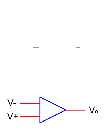
8
In class, you have studied the analysis of op-amp circuits using the ideal op amp model. The ideal op
amp model assumes that there is zero voltage across the two op amp inputs and zero current into those
inputs. A small dc voltage and tiny currents exist at the inputs. In modern op-amps, like the LF411, with
junction field-effect transistor (JFET) input stages, the currents are in the pico-ampere (10
A) range
and can be ignored. The effect of the dc voltage values can be observed when the input signal is set to
zero.
For the op-amp shown in figure 1.3 below, the input offset voltage,
, is defined as the voltage that
must be applied across the + and – inputs so that the output voltage is zero. When the effect of the offset
voltage is considered, and the actual op amp output is given by:
=
(
)
where A = open loop gain of the op amp. Using this equation:
=
If the output is connected directly to the inverting input
(
=
)
, and the non-inverting input is
grounded (
= 0), the equation above becomes:
=
=
1
+ 1
Since 1:
=
. This method will be used in the experiment to measure the input offset
voltage,
, for the op-amp.
Figure 1.3
An inverting op amp amplifier is shown in figure 1.4 below. If we set
= 0, the circuit of figure 1.5
results. In the lab you will observe that under these zero input conditions, a dc output voltage can be
measured. This voltage is due to the offset voltage,
.

9
Figure 1.4
Figure 1.5
PRELIMINARY C
ALCULATIONS
1. An output voltage,
, is measured. Show that
=
1 +
.
Figure 1.6
2. Calculate values for resistors
and
in to produce the following values for voltage gains,
.
)
= 10 )
= 100
Fi
gure 1.7

10
3. Calculate values for resistors
and
to produce the following values for volage gains,
.
)
= 1 )
= 100
Figure 1.8

11
PROCEDURE
PART 1: MEASURING OFFSET VOLTAGE
1. Construct Figure 1.9 and measure the output voltage,
. As discussed in the background
information, this is
.
Figure 1.9
Element
Measured
2. Use
= 33 and
= 3.3. Re-measure the output voltage, V
o
. Using the results of
step 2 above, verify that the output voltage now is
=
1 +
.
Figure 1.10
Element
Measured

12
PART 2: INVERTING GAIN AMPLIFIER
1. Using the resistor values computed in the pre-lab for A
v
= -10. Measure the circuit’s voltage gain by
the following procedure:
Figure 1.11
Element Calculated Measured
2. What is the phase shift between v
i
and v
o
?
Element Measured
Phase Shift

13
3. Measure the -3dB roll-off frequency using the following procedure.
a. Set the scope to display only channel 2,
.
b. Press MEASURE. Record the amplitude of this signal and calculate the amplitude that would be
3dB LESS.
c. Increase the frequency of the signal generator in 10 kHz steps, recording the amplitude of v
o
at
each frequency up to 100 kHz. Record the exact frequency at which the amplitude falls to the –
3dB level.
d. Calculate the gain at each frequency in decibels
(
)
= 20log
. Assume
remains
constant. Graph the gain (in dB) versus frequency and record the gain-bandwidth product,
, for
the amplifier. Use a log scale for the horizontal frequency axis.
Frequency
(
)
Exact Hz
value @ -3dB
level

14
4. Observe the effect of the power supply voltage on the output signal with the following procedure.
a. Return the signal generator to 1 kHz and 100
. Increase the input voltage until v
o
swings
from -10 to +10 volts. In other words, the positive and negative peaks of the output sine wave
are at +10 and -10 volts.
b. Check that the power supply is in the fixed tracking mode. SLOWLY REDUCE the power
supply voltage from ±15 volts to ±5 volts, watching the output.
c. Record the supply voltage at which the output changes. Describe the change.
d. Carefully return the supply voltage to ± 15 volts. DO NOT EXCEED ± 18 volts!
Element
Measured
Supply Voltage
5. Using the resistor values computed in the pre-lab for A
v
= -100. Measure the circuit’s voltage gain
by the following procedure:
6. What is the phase shift between v
i
and v
o
?
Element Measured
Phase Shift

15
7. Measure the -3dB roll-off frequency.
Frequency
(
)
Exact Hz
value @ -3dB
level
8. Observe the effect of the power supply voltage on the output signal.
Element
Measured
Supply
Voltage

16
9. Compare the performance of the two amplifiers as follows:
e. Combine the frequency response graphs from steps 3 and 7 on the same graph.
f. Extend a line through the points A and B, as shown in Figure 1.12. Draw a horizontal line at gain
= 106 dB (this is the open loop gain of this op-amp). Record the frequency where these two lines
intersect. This is f
b
, the open loop gain cutoff frequency.
g. Extend the diagonal line running through A and B. Record the frequency that this line intersects
the 0 dB axis. This is
(
)
, the gain bandwidth product of the op amp.
h. Compare the values obtained in Step 4 from the x10 amplifier and the x100 amplifier. Develop a
relation between the supply voltage and the maximum output signal.
Figure 1.12

17
PART 3: NON-INVERTING GAIN AMPLIFIER
1. Construct the non-inverting gain amplifier with a gain of 1 and apply a sinusoidal signal of
100mV peak to peak (p-p) at 1 kHz. Measure and record the output voltage,
. Calculate and
record the gain of the amplifier.
Figure 1.13
Element Measured
2. Measure and record the phase shift between
and
.
Element Measured
Phase Shift


19
PSPICE: OPERATIONAL AMPLIFIER CIRCUITS
SIMULATIONS FOR LAB REPORTS:
1. Build the inverting amplifier (Figure 1.11) with the same resistors used in the lab for a gain of 10.
Capture the wave forms of
and
. Once you have obtained the values calculate the gain and
compare it to your measured values.
2. Build the inverting amplifier (Figure 1.11) with the same resistors used in the lab for a gain of
100. Capture the wave forms of
and
. Once you have obtained the values calculate the gain
and compare it to your measured values.
3. Simulate the roll off frequency using the AC Sweep function for both gains of 10 and 100 for
Figure 1.11.
4. Build the non-inverting amplifier (Figure 1.13) with the same resistors used in the lab for a gain
of 1. Capture the wave forms of
and
. Once you have obtained the values calculate the gain
and compare it to your measured values.
5. Build the non-inverting amplifier (Figure 1.13) for a gain of 100 with the same resistors used in
the lab. Capture the wave forms of
and
. Once you have obtained the values calculate the
gain and compare it to your measured values.
6. Simulate the roll off frequency using the AC Sweep function for both gains of 10 and 100 for
Figure 1.13. The range of frequencies to sweep should be from 1k to 1MEG, it might be
necessary to extend past a MEG.
Note 1: An operational amplifier model of the LF741 or LF411 op amp used in this experiment is
available in the PSPICE library. It is referred to as LF741 and can be found in the Eval Library in the
demo/student version of PSPICE.
Note 2: DC supplies must be connected to pins 4 and 7 in the PSPICE simulation just as you did in the
laboratory experiment.

20
HOW TO RUN AC SWEEP AND YIELD A DB VS HZ PLOT:
1. Open the simulation profile and change the “Analysis Type” from “Transient” to “AC
Sweep/Noise”.
Figure 1.15
2. Enter your starting frequency and end frequency in the top right corner. Ensure that you have at
least 1000 points per decade, this should give an adequate resolution.
Figure 1.16

21
3. The simulation will yield a voltage on the y-axis and hertz on the x-axis. For the purposes of this
lab it is necessary to change the voltage to decibels.
Figure 1.17
4. Double click the trace name, in this example it’s “V(R5:1)” and located at the origin of the graph.
Figure 1.18

22
5. A dialog box will appear with the “Trace Expression” prepopulated.
Figure 1.19
6. Add “DB()” to the expression. This is a mathematical function that will transform our trace into a
DB scale. Click “OK” when you are done.
Figure 1.20
7. If everything was done correctly the graph will be represented by DB and Hz.
Figure 1.21

23
EXPERIMENT 2: DIODE CHARACTERISTICS
BACKGROUND
The current-voltage characteristics of a diode are given by the equation:
=
1
Where =
(
1
)
= =
(
25.85
3
00
)
=
= 1.38 × 10
°
=
=
= 1
.602 × 10
=
A plot of this characteristic is shown below.
Figure 2.1
To simplify diode circuit analysis and design, a linear diode model is often used to approximate the diode
behavior. The following two models are used here:
Figure 2.2

24
Figure 2.3
PRELIMINARY CALCULATIONS
1. Using the diode current-voltage equation given below with Is = 14.11*10-9 and n = 1.984,
tabulate values of diode current as the diode voltage ranges from -5V to 1.6V. Use increments of
1 V from -5 V to 0 V. Then use increments 0.05 V in the positive voltage range. Assume that the
circuit is operating at 300°K.
=
(
1)
2. U
se the diode equation given above to show that:
ln
(
)
= ln
(
)
+
and
log
= log
+
if ln
=
3. R
eferring to Figure 2.4, assume that
=
cos and sketch
using the following models for
the diode:
a. Ideal diode
b. Piecewise linear diode model with a forward resistance of
and a cut-in voltage of
.
Figure 2.4

25
PROCEDURE
1. Construct the circuit in Figure 2.5 with 1N4002 diode. Apply a DC supply (initially set to zero) for
.
2. Varying the DC power supply voltage from –5 to +1.6V on Figure 2.5, measure and record
,
,
and
, using the multimeter. Calculate the diode current,
. Plot
versus
.
Figure 2.5
()
()
()
()
-5.00
-4.00
-3.00
-2.00
-1.00
0.00
0.01
0.02
0.03
0.04
0.05
0.10
0.15
0.20
0.40
0.60
0.80
1.00
1.20
1.40
1.50
1.60

26
3. Use the curve tracer to obtain another
versus
plot. Your lab instructor will instruct you on the
proper use of the curve tracer. Compare this curve to the one obtained in part 2.
4. Using the data obtained in part 2, re-plot
(log scale) versus
(linear scale). Use only the diode
voltages from 0 to 1.6V. A graph like the one shown in Figure 2.6 should result. Extrapolate the
linear portion of the curve (higher current values) to the y-axis as shown by the dashed line. Use the
resulting y-axis intercept along with the results of the preliminary calculations (2b) to find a value for
. Expected values for
are in the nano-ampere range.
Note: Use Excel on a computer because other software versions will present with issues.
Figure 2.6
Determine the slope of the line extrapolated in part 4 (in log
per volt). Use this slope along with the
results of the preliminary calculations (2b) to find
for your diode. Determine n, assuming VT =
25.6 mV; usually n will be slightly more than 1.
5. Using the values for
and n obtained in parts 4 and 5, write the diode equation for your diode and
plot on the same graph as the results of parts 2. How does this compare to your measured results?
Note: It may be necessary to hand extrapolate to obtain the proper slope.
6. Using the plot from part 2 create a piecewise linear model for your diode by approximating the curve
with two straight lines as shown in the background section. Determine the forward resistance,
, and
the cut-in voltage,
.
7. Build Figure 2.7 and use the oscilloscope to measure and record the input voltage and the resistor
voltage.
Figure 2.7

27
PSPICE: DIODES
1. Use PSPICE to generate the I-V characteristic of the D1N4002 found in the PSPICE library (see
instructions under PSPICE Information).
2. Modify the D1N4002 by changing the value of Is and n to the values measured in parts 4 and 5. Be
sure to save with a different diode name (like D1N4002_mod). Use PSPICE to generate the new I-V
curve. How do the curves generated compare to the data obtained in part 2?
3. Use your modified diode and simulate the circuit in
Figure 2.7. Plot the input voltage and the resistor
voltage. Compare these results to your measurements.
Note: A PSPICE model of the 1N4002 diode used in this experiment is available in the Eval library of
PSPICE. It is referred to as D1N4002. In this experiment you will need to generate an I-V characteristic
of a diode and modify diode parameters. Brief instructions for doing these procedures are given below.
DETERMINATION OF A DIODE I-V CHARACTERISTIC
1. Start a new PSPICE project and enter the schematic shown in Figure 2.8. The diode should be the
D1N4002 from the EVAL library. Use VSRC for the voltage source. Add a current probe at the top
(anode) of the diode.
Figure 2.8
2. To obtain the I-V characteristic of the diode, we want to apply a range of voltages and measure the
corresponding current. The voltage of the source can be varied over a specified range by using the DC
sweep analysis. Start a new simulation profile and name it “DC Sweep”.
3. Select DC Sweep as the Analysis Type and Voltage Source as the Sweep variable. Indicate the name
of your voltage source in the Name box. Note that in Figure 2.8 the example has the source named V1.
This may be different for your schematic.
4. Under Sweep type, select Linear, and enter:
Start Value = -6
End Value = 2
Increment = 0.01
Click “OK”

28
1. Run the simulation. A curve should appear on the display. Select dropdown “Plot” Axis Settings
Y- axis. Choose the data range to be User Defined and set the range to go from 0 to 25 mA. Similarly,
adjust the X-axis range to go from -1 to +1 volts. Your display should appear like the one shown in
Figure 2.9.
Figure 2.9
MODIFYING THE DIODE MODEL
1. Double click on the model name D1N4002 as it appears on the PSPICE schematic. Modify the
name as it appears in the window that appears to D1N4002_lab. Select OK.
2. Highlight the diode device and right click, select Edit PSPICE Model. A model window will
open.
3. A list of model names will appear in the left column of the PSPICE Model window. Select
D1N4002 and modify the name to D1N4002_lab. Click in the right panel and the modified name
should also appear in that listing.
4. Note that all the model parameters of the standard D1N4002 appear. To better model the 1N4002
used in the lab, modify the values of IS and n to match the values that you found in the
experiment (steps 4 and 5).
5. Click the Save Library icon and close the editor window.
6. Re-run the simulation. Note that the IV curve has changed.

29
EXPERIMENT 3: CLIPPER AND CLAMPER CIRCUITS
BACKGROUND
This experiment explores several clipper (also called limiters) and clamper circuits. Clippers and clampers
are important applications of the diode.
A clipper circuit is used to clip off a portion (or portions) of a time varying signal above or below a
specified level. Figure 3.1 illustrates a clipper that limits or clips the positive part of a
signal and figure 3.2 illustrates a clipper that clips the negative part of a signal.
Figure 3.1
Figure 3.2
A clamper circuit adds a dc level to a time varying signal. Clampers are sometimes referred to as
DC restorers. The input-output relationship of a typical clamper circuit is shown in figure 3.3.
Figure 3.3

30
PRELIMINARY CALCULATIONS
1. Refer to the circuit in Figure 3.4. Plot the transfer characteristic (output voltage amplitude versus
the input voltage amplitude) and indicate the positive voltage at which the waveform at
is
clipped. Assume a piecewise linear model for the diode with zero forward resistance and voltage
found in experiment 2.
Figure 3.4
2. Refer to the circuit in Figure 3.5. Plot the transfer characteristic (output voltage amplitude versus
the input voltage amplitude) and indicate the negative voltage at which the waveform at
is
clipped. Assume a piecewise linear model for the diode with zero forward resistance and voltage
found in experiment 2.
Figure 3.5

31
3. Refer to the circuit in Figure 3.6. Plot the transfer characteristic (output voltage amplitude versus
the input voltage amplitude) and indicate the voltages at which the waveform at
is clipped.
Assume piecewise linear models for all the diodes.
Figure 3.6
4. Refer to the circuit in Figure 3.7. Assume a 10V peak to peak, 1 kHz square wave input.
Sketch the output waveform assuming:
a. RC = 2.5ms
b. RC = 0.5ms
Figure 3.7


33
PROCEDURE
1. Construct the single positive peak clipper in Figure 3.9. Using the oscilloscope, measure and
record the level at which the waveform clips on the positive side of the wave form.
Figure 3.9
Measured
2. Construct the negative clipping circuit shown in Figure 3.10. Using the oscilloscope, measure the
level at which the
waveform clips on the negative side of the wave form for each input
voltage. Why does this level change dependent on the amplitude of the input signal?
Figure 3.10
()
()
1
2
3
4

34
3. Construct the zener diode clipper circuit in Figure 3.11. Use the 1N746A zener diode. Using the
oscilloscope, measure the level at which the
waveform clips on the positive and negative sides.
Run a PSPICE simulation of the circuit and test with a 1 kHz sine wave input. Compare the
experimental results with those obtained in the pre-lab. Also compare the results obtained in the
PSPICE simulation. Use the zener diode breakout model in PSPICE as described below.
Figure 3.11
Measured
4. Construct the clamper circuit shown in Figure 3.13.Observe the output waveform,
. Note if the
signal is distorted and to what degree.
Figure 3.12
Measured

35
5. Construct the clamper circuit shown in Figure 3.13.Observe the output waveform,
. Note if the
signal is distorted and to what degree.
Figure 3.13
Measured
6. Set the oscilloscope coupling to DC. Vary the input voltage amplitude slightly and observe that
one side of the sine wave output remains clamped to a fixed voltage. What is that voltage?
Measured
7. Construct the clamper circuit shown in Figure 3.14. Insert the measured values into the following
table.
Figure 3.14
10
0.1
470

36
PSPICE INFORMATION
1. Run a PSPICE simulation of the circuit in Figure 3.9 and compare this to step one of the prelab.
What is the chief source of any discrepancy? For this and all other PSPICE simulations of the
diode use the 1N4002 model in the PSPICE library.
2. Run a PSPICE simulation of the circuit in Figure 3.10 and test with 1 kHz sine wave inputs of
amplitudes used in step 3 and compare with your experimental results. Compare the experimental
results with those obtained in the pre-lab.
3. Run a PSPICE simulation of Figure 3.11 and compare the findings with the lab and prelab.
4. Run a PSPICE simulation of Figure 3.12.
5. Run a PSPICE simulation of Figure 3.13.
6. Run a PSPICE simulation of Figure 3.14 with 10
only.
D
IODE BREAKOUT MODELS
2. In the previous experiment the 1N4002 model was modified to have the parameters measured for
your diode. Sometimes a model for the diode that you are using will not exist in your PSPICE library.
In those cases, you can use a breakout part model to create a model for your device as follows:
3. For a regular diode, use the breakout diode, Dbreak that is included with the BREAKOUT library.
You may need to add this library if you have not used it before.
4. After you have placed the Dbreak component in your circuit, click on the diode and go to Edit
Pspice Model. The model editor will open and display the default diode parameters. You may change
the values of any of the parameters in the window on the right and/or you may add additional PSPICE
parameters that are part of the PSPICE diode model. A list of these parameters can be found in the
PSPICE manual.
5. Save the model and close the Model Editor window.
Note: In the case of a zener diode such as the 1N746A, use DbreakZ, from the Breakout Library. The
approximate zener breakdown voltage is set with the parameters BV and IBV. Using the specification
sheet for a zener diode (or your measurements) we can determine the typical zener breakdown voltage
(BV) and the current at which it occurs (IBV). Thus, to simulate a zener diode with a zener voltage of
10 volts at a current of 20 mA, add the parameters BV = 10 and IBV = 20 mA to the breakout model.
In experiment 2 you measured the zener voltage for the 1N746A.

37
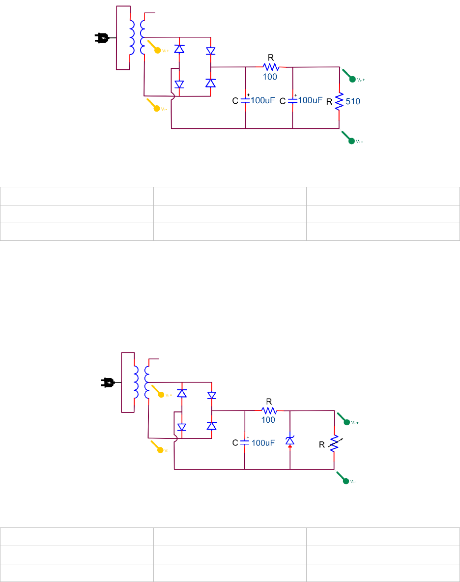
EXPERIMENT 4: POWER SUPPLY CIRCUITS
BACKGROUND
This experiment explores a variety of DC power supply circuits. Generally, a DC power supply converts
the 110V, 60Hz AC voltage from a wall outlet to a constant DC voltage. A typical DC power supply
consists of a rectifier, a filter and a regulator as shown below in Figure 4.1.
Figure 4.1
The rectifier circuit may be a full wave or half wave rectifier. There are a variety of rectifier
configurations that you will discuss in the lecture for this course. The output of the half wave
and full wave rectifiers are shown below in Figure 4.2.
Figure 4.2
The purpose of the filtering circuit is to reduce the fluctuation in the rectifier output and produce a near
constant level DC voltage. Filter circuits may be as simple as a single capacitor, or they may involve a
more complex filter such as a π-filter. The output of the filter will appear as the voltage shown in Figure
4.3.
Figure 4.3

38
From this waveform we can compute the percent ripple as:
()
,
× 100
Filters can reduce the ripple in a power supply, but to further reduce the ripple, a voltage regulator may be
used. In this experiment a voltage regulator employing a zener diode is used.
PRELIMINARY CALCULATIONS
1. The circuits in this experiment use a center-tapped transformer (as shown in Figure 4.5) with a
7.5VAC-RMS output across half of the secondary. What is the peak-peak voltage of the sine wave
corresponding to this RMS voltage?
2. Analyze and calculate
for each circuit in the procedures. Write the calculations in the following.
3. Find the minimum value of load resistance for which the voltage regulator in figure 4.4 will hold a
constant output of 6.8 volts. Assume a 6.8-volt zener is used.
Figure 4.4

39
PROCEDURE
1. Construct the circuit shown in Figure 4.5. Use the 1N4002 diode. Note that you are only applying 7.5
VAC-RMS from the transformer secondary. Use the oscilloscope to observe the voltage,
, at the
transformer and
across the 510Ω load resistor.
Figure 4.5
Calculated
Measured
2. Construct Figure 4.6 , make sure that the polarity of the capacitor is correct. Use the oscilloscope to
observe the output voltage and measure the percentage of ripple on this output.
Figure 4.6
Calculated
Measured
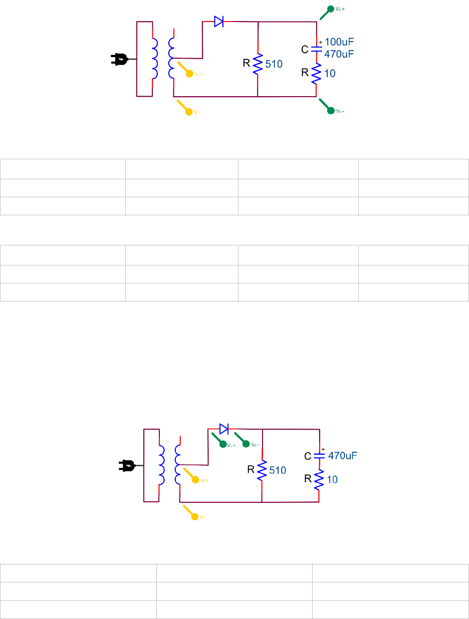
40
3. Construct Figure 4.7 and use the oscilloscope to measure this resistor voltage and the ripple voltage.
Note that this voltage is proportional to the current flowing through the capacitor during charge and
discharge. What is the relationship between the percent ripple and the value of the capacitor used?
Figure 4.7
100
Calculated
Measured
470
Calculated
Measured
4. Construct Figure 4.8. Use the oscilloscope to measure the voltage across the diode in the reverse
direction (positive side of probe on the diode’s cathode) as shown in Figure 4.8. The peak value of
this voltage is referred to as the peak inverse voltage. What is the relationship between this voltage
and the DC voltage produced by the power supply?
Figure 4.8
Calculated
Measured

41
5. Construct the circuit shown in Figure 4.9. Use the oscilloscope to observe the voltage across one half
of the transformer secondary and across the 510Ω load resistor.
Figure 4.9
Calculated
Measured
6. Construct Figure 4.10, ensure that the polarity of the capacitor is correct, Use the oscilloscope to
observe the output voltage and measure the percentage of ripple on this output.
Figure 4.10
Calculated
Measured
42
7. Construct Figure 4.11. Use the oscilloscope to measure this resistor voltage. Note that this voltage is
proportional to the current flowing through the capacitor during charge and discharge.
Figure 4.11
Calculated
Measured
8. Construct Figure 4.12. Note the change in the charge and discharge currents. Measure the output
voltage and compute the ripple. Compare these results to those obtained in parts 2 and 3. What is the
relationship between the percent ripple and the value of the capacitor used?
Figure 4.12
Calculated
Measured
43
9. Construct Figure 4.13 and use the oscilloscope to measure the percent ripple across each of the
capacitors.
Figure 4.13
Calculated
Measured
10. Construct the circuit in Figure 4.14. Use a 1N957A zener diode. Measure the load voltage and percent
ripple with this zener voltage regulator. Decrease the load resistance until the output voltage is no
longer regulated at 6.8 volts. That is, negative going ripple spikes just begin to appear in the output
voltage. Compare this resistor value to the theoretical minimum load resistance found in the pre-lab.
Figure 4.14
Calculated
Measured
44
PSPICE INFORMATION
1. Use PSPICE to simulate the following circuits:
a. Figure 4.6.
b. Figure 4.9
c. Figure 4.10
d. Figure 4.13
e. Figure 4.14
2. Compare your measurements with the results of the simulations. Use the PSPICE model for the
1N4002 and use DbreakZ to model the zener diode. See the section at the end of this experiment for
information on modeling the center-tapped transformer in PSPICE.
3. Compare the percent ripple, peak inverse voltage and charging currents in each circuit.
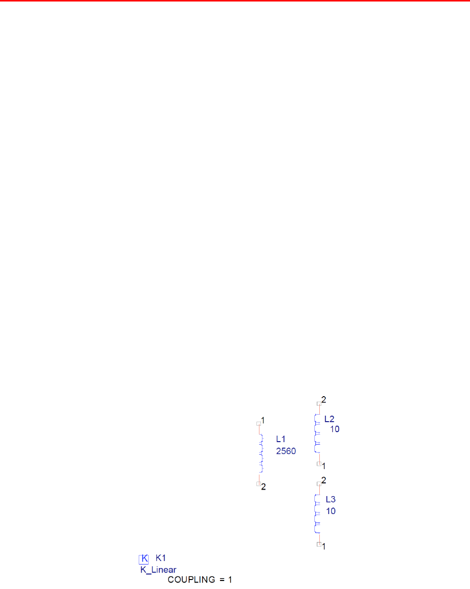
MODELING OF A CENTER-TAPPED TRANSFORMER
In this section we will model the center-tapped transformer used in the experiment with mutually coupled
inductors. The transformer provided has a 120V-rms 60Hz sine wave applied to the primary (input) and
7.5V-rms sine waves across each half of the secondary (output). Thus, the ratio of the input to the output
is 16:1 and a transformer with a turn ratio of 16:1 is needed. This turns ratio can be obtained by making
the values of the inductances proportional to the square of the turn ratio, or 162:1 (256:1). To obtain this
value we will choose the primary inductor to be 2560 H and each of the secondary inductors to be 10H
each.
1. Place three inductors and set their values as shown in Figure 4.15 below. Also, place the part
K_Linear from the Analog Library on the schematic. This part provides the coupling between the
inductors, but it is not actually connected to the circuit.
Figure 4.15

45
2. Double click on the K_Linear part and the Property Editor will open. Tab over to the columns
labeled: L1, L2, L3 and enter the names of the three inductors in those boxes. Note that in this case
the inductors are also named L1, L2, and L3. Select Apply and close the Property Editor.
3. Add the additional components and wire as shown in Figure 4.16. Note that the 120V- rms sinusoidal
input is applied with a 170V peak sine wave.
Figure 4.16
4. Run a transient analysis on this circuit. The output should be an approximately 10.6 volt peak sine
wave. Note that this corresponds to the 7.5V-rms output expected.
NOTE: For some of the circuits only one half of the secondary is used. In those cases, replace the
resistor across the other half with a large resistor (1G for example)

46
EXPERIMENT 5: BIPOLAR JUNCTION TRANSISTORS
BACKGROUND
This experiment investigates the properties of the bipolar junction transistor (BJT). Among the greatest
developments of the 20th Century, this device in all its forms has created a quantum leap in electronics
and technology.
The BJT comes in two main forms: NPN and PNP. These are manufactured in hundreds of different
packaging styles. For this experiment, you will be using the 2N2222A BJT. It is an NPN, general purpose
transistor which comes in two case styles: metal and plastic. Pin outs are shown in the diagrams below.
Transistors can operate in three regions, saturation, active or cut-off. To work as an amplifier with useful
gain, the transistor must be biased into the active or linear region. The point at which the transistor is
biased in this region, along with other circuit parameters, determines the operating Q point, i.e. the
collector current and collector-emitter voltage. These, together with the circuit parameters, determine the
input impedance, output impedance and voltage gain of the amplifier.
To accurately model the operation of a BJT amplifier, PSPICE uses several transistor parameters
specified by the manufacturer. However, some of these parameters can vary over a wide range of values
and are specified as a range in manufacturers’ specifications. PSPICE only uses typical values.
One of the most important parameters in determining the Q point is the transistor’s beta, β or DC forward
current gain. For the 2N2222A, this value can range from 100 to 300 for individual transistors and varies
with temperature and collector current. A design engineer must allow for these variations to ensure the
mass-produced system or device functions to specifications no matter what individual transistors are used.

47
PRELIMINARY CALCULATIONS
1. Using the equations, you have developed in steps 1-4, design amplifiers in each of the three
configurations (Figure 5.2, Figure 5.3, Figure 5.4
)
with the following specifications:
= 8,
=
1
and a = 161. For the transistor use the PSPICE model 2N2222A.
2.
Calculate
,
,
,
, and
.
3.
Develop a DC load line and place the Q-point appropriately.
4. Using PSPICE and the model for the 2N2222A transistor (Q2N2222A in the EVAL library), simulate
each of the three designs and verify their performance to specification.
PROCEDURE
PART 1: MEASURING TRANSISTOR BETA
1.
Construct the circuit in figure 5.1. Measure the voltage across the collector resistor, RC. Because a
1.1 kΩ resistor is used, the voltage will be the collector current,
, in milliamperes. Adjust the 5V
(
) supply to obtain collector currents close to the values specified in the table below. Measure the
voltage across the base resistor,
. Use this value to determine the value of the base current
.
Fi
gure 5.1
=
1.1
Measure
=
100
DC Beta =
0.1mA
0.2mA
0.4mA
0.8mA
1.0mA
2.0mA
4.0mA
2. While in the lab, calculate the beta values for this transistor for use later in the experiment.

48
PART 2: Q-POINT
1. Construct the circuit in Figure 5.2 using the resistor values and power supply voltage calculated in the
pre-lab. Measure the Q-point of the circuit and record the collector-emitter voltage
and collector
current,
.
Figure 5.2
Calculate
Measure
Percent
Error
2. Construct the circuit in Figure 5.3 using the resistor values and power supply voltage calculated in the
pre-lab. Measure the Q-point of the circuit and record the collector-emitter voltage
and collector
current,
.
Figure 5.3
Calculate
Measure
Percent
Error

49
3. Construct the circuit in Figure 5.4 using the resistor values and power supply voltage calculated in the
pre-lab. Measure the Q-point of the circuit and record the collector-emitter voltage
and collector
current,
.
Figure 5.4
Calculate
Measure
Percent
Error
4. Compare the measured results of all the circuits. Using the values of for your two devices compute
the expected values of
for each circuit. Which of the circuits is least sensitive to variations in ?
Which is most sensitive? Does the change in
due to the change in for each circuit correspond to
the change observed in the laboratory?

50
PSPICE INFORMATION
1. Using the procedure below, find the
parameter in the PSPICE model for the Q2N2222 to obtain
the values measured for the transistor provided in the experiment. You may have to adjust the
slightly up or down to get the beta value close to that measured. As a starting point use this equation
to get an approximate value:
=
0.912
1 0.912
14.34 × 10
.
2. Re-simulate the circuits in figures 5.2, 5.3 and 5.4 in PSPICE for both of your value and verify each
circuit’s performance for each device. Compare the results of these simulations to your experimental
results. Also, compare them to the results obtained in the pre-lab simulation with the default .
CHANGING TRANSISTOR MODEL PARAMETERS IN PSPICE
In this example we will modify the Q2N2222/EVAL PSPICE model to produce a DC of 200.
1. Open a new blank project.
2. Place a Q2N2222/EVAL transistor on the schematic.
3. Edit the name of the device in schematic to any name desired. e.g. Q2N2222_mod.
4. With the device highlighted, select PSPICE MODEL under the EDIT pull down menu.
5. Edit the name in the model list from Q2N2222 to the name you have chosen (Q2N2222_mod). Click
on the right window and notice the model name changes there, too.
6. Find
in the text parameters to the right of the edit window. It has a value of 255.9.
7. Change the value of
to the value calculated based on the measured (in this case 378)
8. Save the library and close the Model Editor window.
9.
Place this modified device in the circuit shown in figure 5.3. Set the base current source to the value
required for your Q-point. In our example,
= 1 mA and = 200, thus,
= 5μA.
Fi
gure 5.5
Q1
Q2N2222_mod
V110Vdc
I15u
R1
1k
0

51
3. Start a new simulation and set Select Analysis to Bias Point. Check the Output File Option: Include
detailed bias point information…
4. Run the simulation and enable the bias voltage and current display. Note that the collector current is
0.999 mA, very close to the 1 mA expected.
5. In the Simulation window Select View Output File from the window that opens when the
simulation is complete. Scroll down to the bottom and you should see the following listing:
Note that the DC is 200. Thus, the value of
, used is fine for this device. In some cases, you will need
to adjust
slightly to improve the accuracy of the value.

52
EXPERIMENT 6: DESIGN OF COMMON EMITTER AMPLIFIERS
BACKGROUND
The common emitter amplifier is perhaps the most common use of the transistor. However as seen in the
previous experiment, these amplifiers must work with individual devices with betas spanning a 3:1 range.
In addition, beta is affected by device temperature and the amplifiers must meet other performance
specifications, such as input impedance, output impedance and gain,
over a wide temperature range.
The beta affects both the DC and AC characteristics of a BJT. The relationship between the DC
collector and base currents at the Q point is determined by the DC beta of the device,
where:
=
The AC characteristics of a BJT amplifier (gain, input, and output impedance) are determined using
where:
=
=
The AC and DC beta can be determined from the output characteristic of the device as shown in figure
6.1. Note:
and
should be closer to
by less than
. For example, if
= 1 then
should
be between 0.5mA and 1mA and
should be between 1mA and 1.5mA.
Figure 6.1

53
PRELIMINARY CALCULATIONS
1. Refer to Figure 6.2. Using the 2N2222A transistor, design a common emitter amplifier with the
following specifications:
• Voltage gain
10
•
5
•
10
• Output voltage swing of at least ±5 across 50 load
• Circuit is independent, meaning the Q point does not vary by more than 10% with ranging
from 100 to 300.
•
20
Figure 6.2
Theoretical
Draw a DC load line and ensure to include the Q-point on the line.
2. Model your amplifier in PSPICE. Using the Q2N2222A transistor, set the = 100, using the
formula in the PSPICE information below. Measure the amplifier’s gain, input impedance, output
impedance and output swing. Verify that your design meets the specifications in step 1 before
coming to the lab.
=
0.912
1 0.912
14.34 × 10
.
3. Duplicate the circuit and set the = 300. Measure the amplifier’s gain, input impedance, output
impedance and output swing. Verify that your design meets the specifications in step 1 before
coming to the lab.

54
PROCEDURE
1. Construct Figure 6.3 and measure all the DC voltages.
Figure 6.3
Theoretical
Measured
Percent
Error
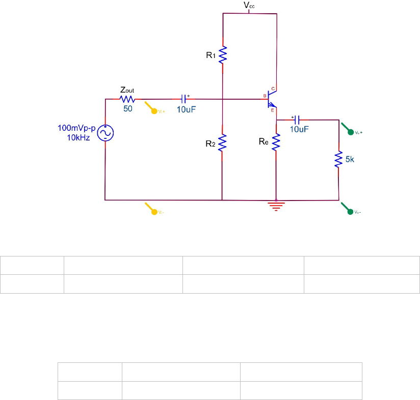
2. Construct the circuit in Figure 6.4 .
Note: Follow the capacitor polarity shown in the figure. Also note that the 50Ω resistor represents the
output impedance of the signal generator and does need to be added to the circuit.
Figure 6.4

55
3. Apply a 400 mVp-p, 1kHz sine wave input to the amplifier. Use the oscilloscope to measure and
record the input and output voltages,
and
. Calculate and record the amplifier’s gain. Compare
the amplifier gain to the one used in the pre-lab.
Figure 6.5
Pspice
Measured
4. Increase the input signal until the output signal shows distortion at the positive or negative peaks.
Verify that the output voltage swing is at least ± 5V. Record the actual values of input and output
voltage where distortion begins.
Pspice
Measured

56
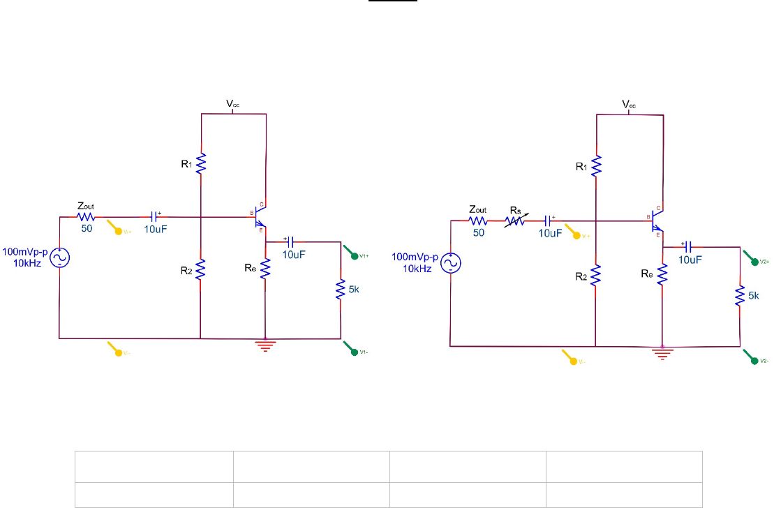
5. Return the signal generator voltage output to 400 mVp-p. Measure and record the output voltage of
the amplifier. This is
. Leaving the signal generator voltage constant, insert increasing resistor
values in series between the generator output and the amplifier input (see Figure 6.6) until the output
of the amplifier drops approximately to one half
. Record this value as
. Calculate the input
impedance of the amplifier using the following equation:
=
Where
= series resistor value. Compare the measured input impedance to the one used in the pre-
lab.
Figure 6.6
Pspice
Measured

57
6. Remove the series resistance and reconnect the signal generator directly to the amplifier input.
Remove the 50KΩ resistor from the amplifier output. Measure and record the amplifier output
voltage. This is
. Place decreasing resistor values, starting at 50KΩ across the amplifier output (see
Figure 6.8) until the output voltage drops to approximately one half
. This output voltage is
. Use
the following equation to calculate the output impedance of the amplifier:
=
(
)
where
= load resistor value. Compare the measured output impedance to the one used in the pre-
lab.
Figure 6.7
Figure 6.8
Pspice
Measured
7. Compile your data and insert it into the table below:
Required
Measured
Calculation
N/A
Met
8. Demonstrate your working amplifier to your lab instructor to verify its performance to specifications.

58
PSPICE INFORMATION
This section discusses a method for finding the voltage gain, input impedance, output impedance, and
output swing of a BJT amplifier using PSPICE. Begin by constructing your schematic with the 2N2222A.
Modify the beta as discussed in Experiment 5 to have the required DC beta. Set a voltage prove to
measure the input waveform and the output waveform.
1. Setting up the Transient Analysis
a. Start a new simulation and select: Time Domain as the Analysis Type
b. Set the “Run to Time” to be long enough to view several cycles of the output.
c. Set the maximum step size to be small enough to view a smooth wave form.
d. Click on the button labeled “output File Options”.
e. A window will open. Check the option “Include detailed bias point”, this will cause the Q
point of the BJT to be displayed in the output file.
f. Click “Ok” to close the simulation settings window.
2. DC Operating Q point
a. Run the simulation.
b. Select ViewOutput File from the output window and a text file will open.
c. Scroll down to view the operating point information for the BJT.
3. Voltage Gain of the Amplifier
a. Select “View”, Simulation Results from the simulation output window.
b. From the “Trace” menu, select “Cursor””Display””Output Curve”. A cross hair
should appear wherever you left click on the curve. A Probe Cursor window will also
appear and display the voltage at the point where the cursor resides. Use the left and or
right arrows to finely adjust the cursor position until it is on the maximum value of the
output curve.
c. Next, we want to set the second cursor on the input curve. Select the symbol for the input
curve at the bottom of the graph. Then right-click on the input curve. The second cursor
should lock on to the input curve. Move this cursor until it resides on the same time value
as the first cursor.
d. These values of the input and output voltage can be used to calculate the voltage gain.
4. Input Impedance of the Amplifier
a. Modify the original schematic to include a resistor to the left of the input capacitor and
insert a voltage probe to the right of the input capacitor.
b. Using the principle of voltage division, we know that when the newly inserted resistor
has a value that is equal to the input impedance of the circuit, the voltage probe will
measure a value that is exactly one-half of the input voltage. Run the simulation with
varying values of the additional resistor until this condition is met.
5. Output Impedance of the Amplifier
a. Remove the resistor that was added for the input impedance calculation and change the
value of the load resistor to 100MEG. This is used to simulate an open circuit since
PSPICE does not allow open circuits. Move the voltage probe to measure the voltage
across this load.
b. Run the simulation and measure the value of the output voltage.
c. Decrease the value of the load resistor until the voltage across it is one-half of the open
circuit value. This resistor value is the output impedance of the amplifier.
59
6. Maximum Symmetric Output Swing
a. Return the load resistance to its original value.
b. Increase the amplitude of the input source until distortion is observed on the output.
c. The value of the output voltage (peak-to-peak) just before distortion occurs is the
maximum symmetric output swing.

60
EXPERIMENT 7: DESIGN OF COMMON BASE AMPLIFIERS
BACKGROUND
The common base amplifier was the original circuit used to demonstrate the gain of the newly invented
transistor in 1948. This form is most used in radio frequency amplification. The low input impedance
makes it ideal for direct connection with 50Ω sources. The word “base” comes from the fact that the first
transistor was a small chip of germanium which had a second piece of doped germanium on top of that.
Two connections to the upper piece were called the emitter and collector. The bottom piece, being at the
bottom of this mini stack, was then the base. Modern transistors do not use this configuration, but the
name has stuck.
PRELIMINARY CALCULATIONS
1. Refer to figure 7.1. Using the 2N2222A transistor, design a common base amplifier with the
following specifications:
• Voltage gain
35
•
=
•
8
• Output voltage swing of at least 3V peak-to-peak across 10KΩ load
• Circuit is independent and the q point does not vary by more than 10% with ranging from
100 to 300
• P
ower supply
20
Fi
gure 7.1
Theoretical

61
Draw a DC load line and ensure to include the Q-point on the line.
2. Model your amplifier in PSPICE. Using the Q2N2222A transistor, set the = 100, using the formula
in the PSPICE information below. Measure the amplifier’s gain, input impedance, output impedance
and output swing, using the PSPICE procedures outlined below. Verify that your design meets the
specifications in step 1 before coming to the lab.
3. Repeat step 2 for a = 300.
PROCEDURE
4. Construct and Figure 7.2 measure all the DC voltages. Use the values calculated in the prelab.
Figure 7.2
Theoretical
Measured
Percent
Error


63
6. Apply a 60 mV peak-to-peak, 10 kHz sine wave input to the amplifier. Use the oscilloscope to
measure and record the input and output voltages. Calculate and record the amplifier’s gain. Compare
the amplifier gain to the one used in the pre-lab.
Figure 7.4
Measured
7. Increase the input signal until the output signal shows distortion. Verify that the output voltage swing
is at least 3V peak-to-peak before hard clipping occurs. Record the actual values of input and output
voltage. Be sure to measure
at the point the signal generator is connected to the circuit. It is more
accurate than trusting the signal generator display.
Measured

64
8. Return the signal generator voltage output to 60 mVp-p. Measure and record the output voltage of the
amplifier. This is
. Leaving the signal generator voltage constant, insert increasing resistor values in
series between the generator output and the amplifier input until the output of the amplifier drops
approximately to one half
. Record this value as
. Calculate the input impedance of the amplifier
using the following equation:
=
50
(
+ 50
)
Figure 7.5
Figure 7.6
Measured

65
9. Remove the series resistance and reconnect the signal generator directly to the amplifier input.
Remove the 10KΩ resistor from the amplifier output. Measure and record the amplifier output
voltage. This is
. Place decreasing resistor values, starting at 50KΩ across the amplifier output until
the output voltage drops to approximately one half
. This output voltage is
, where
= load
resistor value. Compare the measured output impedance to the one used in the pre-lab.
=
(
)
Figure 7.7
Figure 7.8
Measured
10. Compile your data and insert it into the table below:
Required
Measured
Calculation
N/A
Met
11. Demonstrate your working amplifier to your lab instructor to verify its performance to specifications.

66
PSPICE INFORMATION
1. Setting up the Transient Analysis
a. Start a new simulation and select: Time Domain as the Analysis Type.
b. Set the “Run to Time” to be long enough to view several cycles of the output.
c. Set the maximum step size to be small enough to view a smooth wave form.
d. Click on the button labeled “Output File Options”.
e. A window will open. Check the option “Include detailed bias point”, this will cause the Q point
of the BJT to be displayed in the output file.
f. Click ”OK” to close the simulation settings window.
g. DC Operating (Q) Point.
h. Run the simulation.
i. Select View Output File from the output window and a text file will open.
j. Scroll down to view the operating point information for the BJT.
2. Voltage Gain of the Amplifier
a. Select View Simulation Results from the simulation output window.
b. From the Trace menu, select Cursor Display. Then, click on the output curve. A crosshair
should appear wherever you left click on the curve. A Probe Cursor window will also appear and
display the voltage at the point where the cursor resides. Use the left and/or right arrows to finely
adjust the cursor position until it is on the maximum value of the output curve.
c. Next, we want to set the second cursor on the input curve. Select the symbol for the input curve at
the bottom of the graph. Then right-click on the input curve. The second cursor should lock on to
the input curve. Move this cursor until it resides on the same time value as the first cursor.
d. These values of the input and output voltage can be used to calculate the voltage gain.
3. Input Impedance of the Amplifier
a. Modify the original schematic to include a resistor to the left of the input capacitor and insert a
voltage probe to the right of the input capacitor.
b. Using the principle of voltage division, we know that when the newly inserted resistor has a value
that is equal to the input impedance of the circuit, the voltage probe will measure a value that is
exactly one-half of the input voltage. Run the simulation with varying values of the additional
resistor until this condition is met.
4. Output Impedance of the Amplifier
a. Remove the resistor that was added for the input impedance calculation and change the value of
the load resistor to 100MEG. This is used to simulate an open circuit since PSPICE does not
allow open circuits. Move the voltage probe to measure the voltage across this load.
b. Run the simulation and measure the value of the output voltage.
c. Decrease the value of the load resistor until the voltage across it is one-half of the open circuit
value. This resistor value is the output impedance of the amplifier.
67
5. Maximum Symmetric Output Swing
a. Return the load resistance to its original value.
b. Increase the amplitude of the input source until distortion is observed on the output.
c. The value of the output voltage (peak-to-peak) just before distortion occurs is the maximum
symmetric output swing.

68
EXPERIMENT 8: DESIGN OF COMMON COLLECTOR AMPLIFIERS
BACKGROUND
The common collector amplifier is sometimes also called a buffer or emitter follower. Essentially an
impedance transformation circuit, the common collector amplifier is often placed between a common base
or common emitter amplifier and a low impedance device or output, such as 50Ω coaxial cable, a motor,
or a speaker. The common collector amplifier always has a gain less than unity but is still called an
amplifier because it contributes a net power gain to the signal. The common collector amplifier earns its
name as a “buffer” in that it has a high input impedance and a low output impedance. The high input
impedance of the common collector amplifier keeps the low impedance load at its output from reducing
the gain of the previous common emitter or common base stage.
PRELIMINARY CALCULATIONS
1. Refer to Figure 8.1. Using the 2N2222A transistor, design a common collector amplifier with the
following specifications:
• Voltage gain
0.95
•
5k
•
=
• Output voltage swing of at least 2V peak-to-peak across 5KΩ load.
• Circuit is independent and the q point does not vary by more than 10% with ranging from
100 to 300.
• P
ower supply
20
Figure 8.1

69
2. Develop an equation to calculate the amplifier’s input impedance,
. For this step through step 6, the
equations developed must be in terms of circuit components (resistors and capacitors) and the
transistor parameters (
,
and ).
3.
Develop an equation to calculate the amplifier’s output impedance,
. Be sure that the equation
considers the source resistance,
.
4. Develop an equation to calculate the amplifier’s voltage gain,
=
.
5. D
evelop an equation to calculate the amplifier’s current gain,
=
.
6. D
evelop an equation to calculate the amplifier’s power gain,
=
.
7. Model your amplifier in PSPICE. Verify that your design meets the specifications in step 1 for =
100 before coming to the lab.
8. Repeat step 7 for a = 300.


71
2. Apply the power supply with the voltage calculated in the pre-lab. Turn off or disconnect the signal
generator. Measure and record
by measuring the voltage across
. Measure and record
.
Compare your measured Q point to the one used in the pre-lab, refer to Figure 8.3.
Figure 8.3
Theoretical
Measured
Percent
Error
72
3. Apply a 100 mV peak-to-peak, 10 kHz sine wave input to the amplifier. Use the oscilloscope to
measure and record the input and output voltages. Calculate and record the amplifier’s voltage gain.
Compare the amplifier gain to the one calculated in the pre-lab.
Figure 8.4
Measured
4. Increase the input signal until the output signal shows distortion. Verify that the output voltage swing
is at least 2V peak-to-peak before hard clipping occurs. Record the actual values of input and output
voltage.
Measured
73
5. Return the signal generator voltage output to 100 mVp-p. Measure and record the output voltage of
the amplifier. This is
. Leaving the signal generator voltage constant, insert increasing resistor
values in series between the generator output and the amplifier input (see Figure 8.6) until the output
of the amplifier drops approximately to one half
. Record this value as
. Calculate the input
impedance of the amplifier using the following equation:
=
Where
= series resistor value. Compare the measured input impedance to the one used in the pre-
lab.
Figure 8.5
Figure 8.6
Measured

74
6. Remove the series resistance and reconnect the signal generator directly to the amplifier input.
Remove the 5KΩ resistor from the amplifier output. Measure and record the amplifier output voltage.
This is
. Replace
with different values (see Figure 8.8) until the output voltage drops to
approximately one half
. This output voltage is
. Use the following equation to calculate the
output impedance of the amplifier:
=
(
)
where
= load resistor value. Compare the measured output impedance to the one used in the pre-
lab.
Figure 8.7
Figure 8.8
Measured
7. Using the measurements from steps 3 and 5, calculate the amplifier’s current and power gains.
8. Demonstrate your working amplifier to your lab instructor to verify its performance to specifications.

75
9. Replace
with the following values: 10, 50, 100, 200, 1000. With each resistor, measure
and
calculate the output power to the load. Plot the output power versus the load resistance. What load has
the most power delivered to it? Explain the results.
Figure 8.9
Resistor
10Ω
50Ω
100Ω
200Ω
1KΩ

76
10. Place a 6.8KΩ resistor in series with the input capacitor. Measure the output impedance of the
amplifier with this additional source resistance. Use the results of step 3 of the pre-lab to explain the
results.
Figure 8.10
11. Compile your data and insert it into the table below:
Required
Measured
Calculation
N/A
Met

77
PSPICE INFORMATION
1. Setting up the Transient Analysis
a. Start a new simulation and select: Time Domain as the Analysis Type.
b. Set the “Run to Time” to be long enough to view several cycles of the output.
c. Set the maximum step size to be small enough to view a smooth wave form.
d. Click on the button labeled “Output File Options”.
e. A window will open. Check the option “Include detailed bias point”, this will cause the Q point
of the BJT to be displayed in the output file.
f. Click ”OK” to close the simulation settings window.
2. DC Operating (Q) Point
a. Run the simulation
b. Select View Output File from the output window and a text file will open.
c. Scroll down to view the operating point information for the BJT.
3. Voltage Gain of the Amplifier
a. Select View Simulation Results from the simulation output window.
b. From the Trace menu, select Cursor Display. Then, click on the output curve. A crosshair
should appear wherever you left click on the curve. A Probe Cursor window will also appear and
display the voltage at the point where the cursor resides. Use the left and/or right arrows to finely
adjust the cursor position until it is on the maximum value of the output curve.
c. Next, we want to set the second cursor on the input curve. Select the symbol for the input curve at
the bottom of the graph. Then right-click on the input curve. The second cursor should lock on to
the input curve. Move this cursor until it resides on the same time value as the first cursor.
d. These values of the input and output voltage can be used to calculate the voltage gain.
4. Input Impedance of the Amplifier
a. Modify the original schematic to include a resistor to the left of the input capacitor and insert a
voltage probe to the right of the input capacitor.
b. Using the principle of voltage division, we know that when the newly inserted resistor has a value
that is equal to the input impedance of the circuit, the voltage probe will measure a value that is
exactly one-half of the input voltage. Run the simulation with varying values of the additional
resistor until this condition is met.
5. Output Impedance of the Amplifier
a. Remove the resistor that was added for the input impedance calculation and change the value of
the load resistor to 100MEG. This is used to simulate an open circuit since PSPICE does not
allow open circuits. Move the voltage probe to measure the voltage across this load.
b. Run the simulation and measure the value of the output voltage.
c. Decrease the value of the load resistor until the voltage across it is one-half of the open circuit
value. This resistor value is the output impedance of the amplifier.
78
6. Maximum Symmetric Output Swing
a. Return the load resistance to its original value.
b. Increase the amplitude of the input source until distortion is observed on the output.
c. The value of the output voltage (peak-to-peak) just before distortion occurs is the maximum
symmetric output swing.
79
EXPERIMENT 9: MOSFET CHARACTERISTICS AND DC BIASING
BACKGROUND
MOS transistors are used in all significant digital designs, mixed-signal designs, amplifier designs, etc.
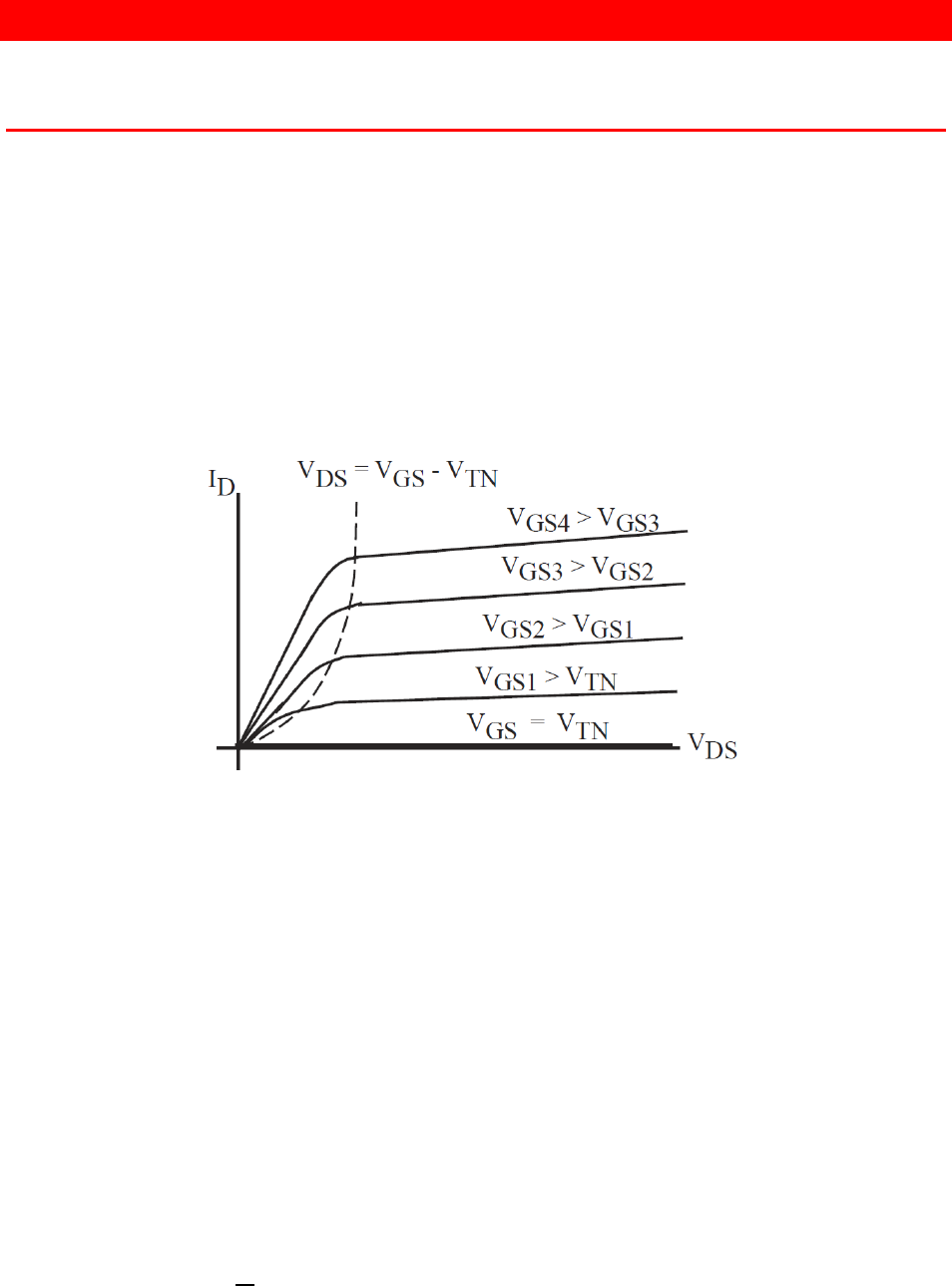
The I-V output characteristics for an N-channel MOSFET are shown in figure 9.1. Note that
is
essentially zero unless the gate voltage exceeds a threshold voltage known as
. The threshold voltage
makes a conductive path between the source and drain by the strong inversion channel formation. In the
case of the N channel MOSFET in figure 9.1, the region to the right of the locus of the equation
=
is called the saturation region. In this region the drain current
depends mainly on the gate-
to-source voltage
. Thus, the transistor behaves as a constant current source or the curve shows a
constant current region that is now independent on the value of
. The left of the locus of the equation
is the triode region, where the curve shows a linear incremental change of
current with increment of
voltage to maintain linear resistance across the source and drain terminals at low
voltages.
Fi
gure 9.1
I
n the saturation region, the current
is expressed by following equation:
=
(
)
Where
=
=
T
he test circuit shown in figure 9.2 can be used to measure the I-V output characteristics for a
M
OSFET. If the oscilloscope is placed in the XY mode, it will display the channel 1 voltage on the x-axis
and the channel 2 voltage on the y-axis. If we invert the channel 1 voltage, the x-axis voltage will
correspond to
. If we divide the channel 2 voltage by 100, the y-axis will correspond to I
. Thus, if
we apply a voltage
>
, the corresponding display will be the
I-V output characteristic for this value of
.
For each value of
, the drain current reaches a near constant value in the saturation region. A plot of
the saturation values of
versus
lie on a straight line, except for very small and very large values

80
of
. As shown in figure 9.3, the straight line drawn through these points intercepts the x-axis at the
threshold voltage
. The slope of the straight line is equal to the square root of the conduction
parameter,
.
Figure 9.2
ID is not constant in the saturation region but increases slightly with increasing
. The output
resistance,
, of the MOSFET is determined from the slope of the I-V output characteristic as shown in
Figure 9.3. Note that
changes with
.
Figure 9.3


82
2. Calculate the resistor values for a second design with the same Q-point. However,
= 1800.
Figure 9.5
3. Use PSPICE to simulate the design found in step 1. Use KP =.012, W = 10u, L = 1u, VTO = 2.1, to
simulate the
and
parameters given in step 1. Note the Q-point values,
and
.
4. Repeat step 3 with KP =.0026, W = 10u, L = 1u and VTO = 0.8, the minimum values of these
parameters for the 2N7000. Note the Q-point values,
and
.
5. Repeat step 3 with KP =.018, W = 10u, L = 1u and VTO = 3, the maximum values of these
parameters for the 2N7000. Note the Q-point values,
and
. Steps 4 and 5 provide the worst-case
analysis for your design. Step 3 provides the nominal design.
6. Repeat steps 3 through 5 with resistor values for the second design found in step 2. How does
affect the stability of the circuit?

83
PROCEDURE
1. Construct the first design of the circuit shown in Figure 9.4, using the resistor values found in step 1
of the pre-lab. Apply a
of 15V. Measure and record the Q-point,
and
. Replace the 2N7000
with the second device. Measure and record the Q-point,
and
.
Figure 9.6
Theoretical
Measured
Percent
Error

84
2. Construct the second design of the circuit shown in Figure 9.4, using the resistor values found in step
2 of the pre-lab. Apply a
of 15V. Measure and record the Q-point,
and
. Measure and record
the Q-point,
and
.
Figure 9.7
Theoretical
Measured
Percent
Error
3. Compare the Q-points calculated in the pre-lab with those measured in steps 1 and 2.
4. In your conclusion discuss the effect of
on Q-point stability. Include in your conclusion a
discussion of how Q-point stability in MOSFETs compares to the same circuit. Which is more stable?
Why?

85
PSPICE INFORMATION
Modeling an N-channel MOSFET
There are several models that can be used to describe the physical characteristics of a MOSFET within
PSPICE. These different models are specified with a “level” number. In this tutorial we will use the Level
1 model, which is the simplest and the default value.
The behavior of a MOSFET device in the saturation region is characterized by the equation:
=
(
)
I
n the level 1 model we can specify the values of VTN (as VTO), k’N (as KP), L and W along with other
parameters that are described in the PSPICE Reference Manual. We will use the breakout model for the
2N7000 since its model is not available in the free version of PSPICE.
Use the breakout model MbreakN3 for the MOSFET. This breakout model is an enhancement type
NMOS device with the substrate connected to the source. Modify the .model statement of
the breakout model as shown in the figure below. For example, if we want to model a device
with KN = 0.25 mA/V and VTN = 1V we could use the parameters shown below. With this statement we
have specified an NMOS device with a VTN =1 volt = VTO.
The Q-point of the MOSFET can be found by simulating the circuit as follows. Select Analysis Type:
Bias Point and check the box next to “Include detailed bias point information…”. Run the simulation and
when it is complete select View Output File. Scroll down to the operating point information provided.

86
EXPERIMENT 10: DESIGN OF COMMON SOURCE AMPLIFIERS
BACKGROUND
The behavior of the MOSFET as an amplifier is analogous to the BJT. Both are three terminal devices
whose input voltage controls the output current source. However, the MOSFET offers the advantage that
no input current is required to either bias or drive the device as an amplifier. Consequently, it does not
present a load to the signal source or previous stage outside of the bias resistors.
Another difference is that the MOSFET operates with a square law relation between the input voltage and
output current, while the BJT has an exponential relationship. This leads to lower values for gm. In other
words, VGS varies significantly for a given output current in the MOSFET, while VBE remains relatively
constant in the BJT.
PRELIMINARY CALCULATIONS
1. Calculate the resistors needed to design the MOSFET common source amplifier in Figure 10.1 with
the following specifications:
•
70
• •
100
• •
20
• •
6
• •
20
Figure 10.1
Design the amplifier to work TO SPECIFICATION with the 2N7000 device parameters measured
in the previous lab.
2. Verify the performance of the amplifier to specification in PSPICE, using the MOSFET breakout
model with the parameters measured in the previous lab. NOTE: If your amplifier fails to work to
specification, REDESIGN IT.

87
PROCEDURE
1. Measure the
of your two devices using the circuit in Figure 10.2 and the following procedure.
Figure 10.2
a. Make sure your signal generator output is set to Hi-Z.
b. Place a voltmeter across
and adjust
so that
equals 0.5mA. (
=
).
Figure 10.3
c. Set the signal generator to produce a 100 mV p-p, 1 kHz sine wave.
d. Set the oscilloscope vertical gain to 200 mV/division.

88
e. Read the peak-to-peak signal,
.
Figure 10.4
f. Record the
= 0.01(
). For example, Vo= 1.20 V. Then
= 1.2(0.01) = 0.012.
g. Repeat steps b through f for
currents of 1, 2, 3, 4, and 5 mA.
h. Graph the data as
versus
. for both devices. You will use this data in subsequent
experiments. Note: This will not be a linear curve.
=
2
= 0.01
0.5mA
1 mA
2 mA
3 mA
4 mA
5 mA

89
2. Construct the circuit in Figure 10.5 using the resistor values calculated in the pre-lab. Measure and
record
by measuring the voltage across
. Measure and record
. Compare your measured Q
point to the one used in the pre-lab.
Figure 10.5
Theoretical
Measured
Percent Error

90
3. Apply a 50 mV p-p, 1kHz sine wave input to the amplifier. Use the oscilloscope to measure and
record the input and output voltages. Calculate and record the amplifier’s gain. Compare the amplifier
gain to the one used in the pre-lab.
Figure 10.6
Measured
4. Increase the input signal until the output signal shows distortion. Verify that the output voltage swing
is at least ± 3V. Record the actual values of input and output voltage where distortion begins.
Measured

91
5. Return the signal generator voltage output to 50 mV p-p. Measure and record the output voltage of
the amplifier. This is
. Leaving the signal generator voltage constant, insert increasing resistor
values in series between the generator output and the amplifier input until the output of the amplifier
drops approximately to one half
. Record this value as
. Calculate the input impedance of the
amplifier using the following equation:
=
(
)
Measured
Figure 10.7
Figure 10.8
Specification

92
6. Remove the series resistance and reconnect the signal generator directly to the amplifier input.
Remove the 50KΩ resistor from the amplifier output. Measure and record the amplifier output
voltage. This is
. Place decreasing resistor values, starting at 50KΩ across the amplifier output (
)
until the output voltage drops to approximately one half
. Use the following equation to calculate
the output impedance of the amplifier:
=
(
)
Measured
Figure 10.9
Figure 10.10
Specification

93
7. Reconnect the 50KΩ load resistor and apply a 50mV p-p sine wave signal at 1kHz to the amplifier.
Note the value of the output voltage. Calculate the voltage value that would be 3dB LESS than this
value. Slowly lower the signal generator frequency until the output voltage reaches this value. Record
the frequency.
Sample Point
Frequency
Voltage
1
2
3
4
5
6
7
8
9
10
8. Compile your data and insert it into the table below:
Required
Measured
Calculation
N/A
Met
9. Demonstrate your working amplifier to your lab instructor to verify its performance to specifications.

94
PSPICE
For Figure 10.1 find the following values in PSPICE.
a. DC Operating Q point
a. Run the simulation.
b. Select ViewOutput File from the output window and a text file will open.
c. Scroll down to view the operating point information for the MOSFET.
b. Voltage Gain of the Amplifier
c. Input Impedance of the Amplifier
d. Output Impedance of the Amplifier
e. Maximum Symmetric Output Swing

95
EXPERIMENT 11: DESIGN OF COMMON GATE AMPLIFIERS
BACKGROUND
The common gate amplifier shares many of the properties of its BJT cousin, the common base amplifier:
low input impedance, high gain, and high output impedance. In addition, it has the same advantages as a
high frequency amplifier as the common base: low feedback capacitance and excellent isolation between
the output and the input. These will be discussed later in this course.
There is one important difference, however. The impedance to ground at the gate is not very critical for
the operation of the common gate amplifier. In the common base version, the base to ground impedance is
crucial in the determining the input impedance and gain.
PRELIMINARY CALCULATIONS
1. Refer to Figure 11.1. Using the 2N7000 MOSFET, design a common gate amplifier with the
following specifications:
Figure 11.1
•
25
•
= 150 ± 20%
•
= 8
• Output voltage swing of at least 3V peak-to-peak across 10KΩ load
• Power supply
< 20.
• Calculate your design using the nominal parameters of
= 0.06
and
= 2.1
2. Model your amplifier in PSPICE. Using the MOSFET breakout model, set
= 0.012, W =
10u, L = 1u and
= 2.1. Measure the amplifier’s gain, input impedance, output impedance and
output swing, using the PSPICE procedures outlined previously. Verify that your design meets the
specifications in step 1 before coming to the lab. If it does not, REDESIGN IT.
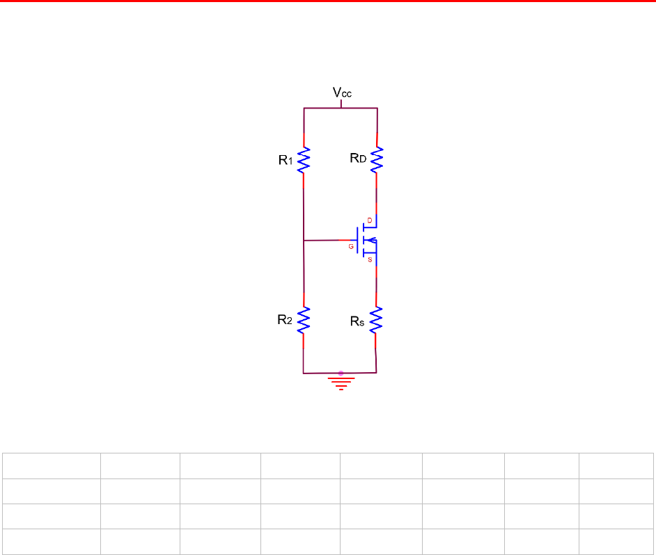
96
PROCEDURE
1. Construct the circuit in Figure 11.2 using the resistor values calculated in the pre-lab. Measure
and record
by measuring the voltage across
. Measure and record
. Compare your
measured Q point to the one used in the pre-lab.
Figure 11.2
Theoretical
Measured
Percent Error

97
2. Apply a 50 mV peak-to-peak, 10 kHz sine wave input to the amplifier. Use the oscilloscope to
measure and record the input and output voltages. Calculate and record the amplifier’s gain. Compare
the amplifier gain to the one used in the pre-lab.
Figure 11.3
Measured
3. Increase the input signal until the output signal shows distortion. Verify that the output voltage swing
is at least 3V peak-to-peak before hard clipping occurs. Record the actual values of the input and
output voltages.
Measured

98
5. Return the signal generator voltage output to 50 mVp-p. Measure and record the output voltage of the
amplifier. This is
. Leaving the signal generator voltage constant, insert increasing resistor values in
series between the generator output and the amplifier input (see Figure 11.5) until the output of the
amplifier drops approximately to one half
. Record this value as
. Calculate the input impedance
of the amplifier using the following equation:
=
(
50 +
)
50
Measured
Figure 11.4
Figure 11.5
Specification

99
6. Remove the series resistance and reconnect the signal generator directly to the amplifier input.
Remove the 50KΩ resistor from the amplifier output. Measure and record the amplifier output
voltage. This is
. Place decreasing resistor values, starting at 50KΩ across the amplifier output (see
Figure 11.7) until the output voltage drops to approximately one half
. This output voltage is
.
Use the following equation to calculate the output impedance of the amplifier:
=
(
)
Measured
Figure 11.6
Figure 11.7
Specification
7. Compile your data and insert it into the table below:
Required
Measured
Calculation
N/A
Met
8. Demonstrate your working amplifier to your lab instructor to verify its performance to specifications.

100
PSPICE INFORMATION
For Figure 10.1 find the following values in PSPICE.
a. DC Operating Q point
a. Run the simulation.
b. Select ViewOutput File from the output window and a text file will open.
c. Scroll down to view the operating point information for the MOSFET.
b. Voltage Gain of the Amplifier
c. Input Impedance of the Amplifier
d. Output Impedance of the Amplifier
e. Maximum Symmetric Output Swing

101
EXPERIMENT 12: DESIGN OF COMMON DRAIN AMPLIFIERS
BACKGROUND
The common drain amplifier is also called a buffer. It does a better job at this than the common collector
amplifier. Although the output impedance of the common drain amplifier tends to be higher than the
common emitter version for a given DC current Q-point, the input impedance is totally independent of the
load. In fact, the output could be shorted to ground, and the input impedance would remain the same. For
this reason, the common drain amplifier is very popular in isolating circuits sensitive to loading, such as
high stability oscillators. In addition, the common drain amplifier can be followed by a common emitter
amplifier, combining high impedance input with high gain to make a versatile circuit with few
components.
PRELIMINARY CALCULATIONS
1. Refer to Figure 12.1. Using the 2N7000 MOSFET, design a common drain amplifier with the
following specifications:
•
= 50
•
= 150 ± 20%
• Voltage gain,
0.95 with a 5KΩ load
• Output voltage swing of at least 2V peak-to-peak across 5KΩ load
• Power supply
20
• Base your calculations on the nominal parameters for the 2N7000 of
= 0.06
and
=
2.1
.
Figure 12.1

102
2. Develop an equation to calculate the amplifier’s input impedance,
. For this step and all steps
through step 6, the equations must be in terms of the circuit component values (resistors or
capacitors), the device parameters (
,
) and the Q point (
,
).
3. Develop an equation to calculate the amplifier’s output impedance,
.
4. Develop an equation to calculate the amplifier’s voltage gain,
=
.
5. Develop an equation to calculate the amplifier’s current gain,
=
.
6. Develop an equation to calculate the amplifier’s power gain,
=
(
)
(
)
.
7. Model your amplifier in PSPICE. Verify that your design meets the specifications in step 1 for
= 0.012, W = 10u, L = 1u and
= 2.1 before coming to the lab.
8. Ensure that your design will meet specification by adjusting your design Q-point using the
values measured for your devices in Experiment 10.

103
PROCEDURE
1. Construct the circuit in figure 12.1. Measure and record
by measuring the voltage across
.
Measure and record
. Compare your measured Q-point to the one used in the pre-lab.
Fi
gure 12.2
Theoretical
Measured
Percent Error

104
2. Apply a 100 mV peak-to-peak, 10 kHz sine wave input to the amplifier. Use the oscilloscope to
measure and record the input and output voltages. Calculate and record the amplifier’s voltage
gain. Compare the amplifier gain to the one calculated in the pre-lab.
Figure 12.3
Measured
3. Increase the input signal until the output signal shows distortion. Verify that the output voltage
swing is at least 2V peak-to-peak before hard clipping occurs. Record the actual values of the
input and output voltages.
Measured

105
4. Return the signal generator voltage output to 100 mVp-p. Measure and record the output voltage
of the amplifier. This is
. Leaving the signal generator voltage constant, insert increasing
resistor values in series between the generator output and the amplifier input (see Figure 12.5)
until the output of the amplifier drops approximately to one half
. Record this value as
.
Compare the measured input impedance to the one calculated in the pre-lab. Calculate the input
impedance of the amplifier using the following equation:
=
Measured
Figure 12.4
Figure 12.5

106
5. Remove the series resistance and reconnect the signal generator directly to the amplifier input.
Remove the 5KΩ resistor from the amplifier output. Measure and record the amplifier output
voltage. This is
. Place decreasing resistor values, starting at 1KΩ across the amplifier output
(see Figure 12.7) until the output voltage drops to approximately one half
. Compare the
measured output impedance to the one used in the pre-lab. This output voltage is
. Use the
following equation to calculate the output impedance of the amplifier:
=
(
)
Measured
Figure 12.6
Figure 12.7
6. Using the measurements from steps 3 and 5, calculate the amplifier’s current and power gains.
7. Demonstrate your working amplifier to your lab instructor to verify its performance to
specifications.

107
8. Apply a 10 kHz, 100mV peak-to-peak sine wave to the amplifier input. Replace the 5KΩ load
resistor with the following values: 10, 50, 100, 200, 1000. With each resistor, measure
and
calculate the output power to the load. Plot the output power versus the load resistance. Which
value receives the maximum power? Explain the results.
Figure 12.8
Resistor
10Ω
50Ω
100Ω
200Ω
1KΩ
9. Place a 6.8KΩ resistor in series with the input capacitor. Measure the output impedance of the
amplifier with this additional source resistance. Use the results of step 3 of the pre-lab to explain
the results. In your conclusion, compare this result with that obtained with the BJT.
10. Compile your data and insert it into the table below:
Required
Measured
Calculation
N/A
Met

108
PSPICE INFORMATION
1. Refer to Experiment 6 for PSPICE information relevant to this experiment.

109
EXPERIMENT 13: DESIGN OF MULTISTAGE AMPLIFIERS
BACKGROUND
Previous labs have explored the strengths and weaknesses of various amplifier circuits. In practice, it is
often difficult to meet all the specifications in a particular application with a single stage, configuration,
or device. For example, voltage gains in the thousands are often required. It is impossible to achieve such
high gains in a single common emitter or common source amplifier. In addition, input and output
impedance requirements may directly conflict with the gain specification.
Multistage Amplifiers offer the designer a way to meet all specifications with various stages providing
gain and others providing the desired impedance characteristics.
In AC coupled stages, the overall frequency response of the multistage amplifier is a function the
individual response of each stage and that stage coupled to the next.
PRELIMINARY CALCULATIONS
1. Using BOTH the 2N7000 MOSFET and the 2N2222A BJT, design a multistage amplifier (at
least two active stages) with the following specifications:
•
100
•
= 620± 10%
• Voltage gain,
5 with a 620Ω load
• Output voltage swing of at least 1V peak-to-peak across 620Ω load
• Power supply
= 20
• Low end cutoff frequency ≤ 40 Hz. You may use any configuration you wish.
2. Ensure that your design will meet specification by modeling the circuit in PSPICE. Use the
measured parameter values (beta,
,
, etc.) for your devices determined in the previous
labs. If your design does not meet ALL specifications, REDESIGN IT. Use standard value
resistors and capacitors. Also note the Q-point of each of the devices in your design.
PROCEDURE
1. Construct your design in the lab. Apply the design power supply voltage. Measure and record the
Q-points of each of the devices in the circuit. Compare these with the values from PSPICE in the
pre-lab.
2. Apply a 100 mV peak-to-peak, 1 kHz sine wave input to the amplifier. Use the oscilloscope to
measure and record the input and output voltages. Calculate and record the amplifier’s voltage
gain. Compare the amplifier gain to the one calculated in the pre-lab.
Measured

110
3. Calculate the output voltage that is 3dB LESS than that measured in step 2. Slowly lower the
signal generator frequency until the output voltage falls to this level. At various frequency
intervals, record the output voltage. Use this data to graph the frequency response of the
amplifier on log-log coordinates. Record the frequency where the output voltage falls by 3dB.
Sample Point
Frequency
Voltage
1
2
3
4
5
6
7
8
9
10
4. Return the signal generator frequency to 1 kHz. Increase the input signal until the output signal
shows distortion. Verify that the output voltage swing is at least 1V peak-to-peak before hard
clipping occurs. Record the actual values of input and output voltage.
Measured
5. Use the method described in experiment 6 to measure the input impedance of your amplifier.
Compare the measured input impedance to the one calculated in the pre-lab.
Measured
6. Use the method described in experiment 6 to measure the output impedance of your amplifier,
starting with RL= 1000. Compare the measured output impedance to the one used in the pre-lab.
Measured

111
7. Using the measurements from steps 2 and 5, calculate the amplifier’s current and power gains.
8. Compile your data and insert it into the table below:
Required
Measured
Calculation
N/A
Met
9. Demonstrate your working amplifier to your lab instructor to verify its performance to
specifications.
10. In your report, describe the design process in detail: why you made certain choices, tradeoffs,
etc. to meet each specification. In your conclusion discuss how well these choices worked
