
© 2009 Microchip Technology Inc. Preliminary DS41338C
MCV14A
Data Sheet
14-Pin, 8-Bit Flash Microcontroller

DS41338C-page 2 Preliminary © 2009 Microchip Technology Inc.
Information contained in this publication regarding device
applications and the like is provided only for your convenience
and may be superseded by updates. It is your responsibility to
ensure that your application meets with your specifications.
MICROCHIP MAKES NO REPRESENTATIONS OR
WARRANTIES OF ANY KIND WHETHER EXPRESS OR
IMPLIED, WRITTEN OR ORAL, STATUTORY OR
OTHERWISE, RELATED TO THE INFORMATION,
INCLUDING BUT NOT LIMITED TO ITS CONDITION,
QUALITY, PERFORMANCE, MERCHANTABILITY OR
FITNESS FOR PURPOSE. Microchip disclaims all liability
arising from this information and its use. Use of Microchip
devices in life support and/or safety applications is entirely at
the buyer’s risk, and the buyer agrees to defend, indemnify and
hold harmless Microchip from any and all damages, claims,
suits, or expenses resulting from such use. No licenses are
conveyed, implicitly or otherwise, under any Microchip
intellectual property rights.
Trademarks
The Microchip name and logo, the Microchip logo, dsPIC,
K
EELOQ, KEELOQ logo, MPLAB, PIC, PICmicro, PICSTART,
rfPIC and UNI/O are registered trademarks of Microchip
Technology Incorporated in the U.S.A. and other countries.
FilterLab, Hampshire, HI-TECH C, Linear Active Thermistor,
MXDEV, MXLAB, SEEVAL and The Embedded Control
Solutions Company are registered trademarks of Microchip
Technology Incorporated in the U.S.A.
Analog-for-the-Digital Age, Application Maestro, CodeGuard,
dsPICDEM, dsPICDEM.net, dsPICworks, dsSPEAK, ECAN,
ECONOMONITOR, FanSense, HI-TIDE, In-Circuit Serial
Programming, ICSP, Mindi, MiWi, MPASM, MPLAB Certified
logo, MPLIB, MPLINK, mTouch, Octopus, Omniscient Code
Generation, PICC, PICC-18, PICDEM, PICDEM.net, PICkit,
PICtail, PIC
32
logo, REAL ICE, rfLAB, Select Mode, Total
Endurance, TSHARC, UniWinDriver, WiperLock and ZENA
are trademarks of Microchip Technology Incorporated in the
U.S.A. and other countries.
SQTP is a service mark of Microchip Technology Incorporated
in the U.S.A.
All other trademarks mentioned herein are property of their
respective companies.
© 2009, Microchip Technology Incorporated, Printed in the
U.S.A., All Rights Reserved.
Printed on recycled paper.
Note the following details of the code protection feature on Microchip devices:
• Microchip products meet the specification contained in their particular Microchip Data Sheet.
• Microchip believes that its family of products is one of the most secure families of its kind on the market today, when used in the
intended manner and under normal conditions.
• There are dishonest and possibly illegal methods used to breach the code protection feature. All of these methods, to our
knowledge, require using the Microchip products in a manner outside the operating specifications contained in Microchip’s Data
Sheets. Most likely, the person doing so is engaged in theft of intellectual property.
• Microchip is willing to work with the customer who is concerned about the integrity of their code.
• Neither Microchip nor any other semiconductor manufacturer can guarantee the security of their code. Code protection does not
mean that we are guaranteeing the product as “unbreakable.”
Code protection is constantly evolving. We at Microchip are committed to continuously improving the code protection features of our
products. Attempts to break Microchip’s code protection feature may be a violation of the Digital Millennium Copyright Act. If such acts
allow unauthorized access to your software or other copyrighted work, you may have a right to sue for relief under that Act.
Microchip received ISO/TS-16949:2002 certification for its worldwide
headquarters, design and wafer fabrication facilities in Chandler and
Tempe, Arizona; Gresham, Oregon and design centers in California
and India. The Company’s quality system processes and procedures
are for its PIC
®
MCUs and dsPIC
®
DSCs, KEELOQ
®
code hopping
devices, Serial EEPROMs, microperipherals, nonvolatile memory and
analog products. In addition, Microchip’s quality system for the design
and manufacture of development systems is ISO 9001:2000 certified.

© 2009 Microchip Technology Inc. Preliminary DS41338C-page 3
MCV14A
High-Performance RISC CPU:
• Only 33 Single-Word Instructions
• All Single-Cycle Instructions except for Program
Branches which are Two-Cycle
• Two-Level Deep Hardware Stack
• Direct, Indirect and Relative Addressing modes
for Data and Instructions
• Operating Speed:
- DC – 20 MHz crystal oscillator
- DC – 200 ns instruction cycle
• On-chip Flash Program Memory
- 1024 x 12
• General Purpose Registers (SRAM)
-67 x 8
• Flash Data Memory
-64 x 8
Special Microcontroller Features:
• 8 MHz Precision Internal Oscillator
- Factory calibrated to ±1%
• In-Circuit Serial Programming™ (ICSP™)
• In-Circuit Debugging (ICD) Support
• Power-On Reset (POR)
• Device Reset Timer (DRT)
• Watchdog Timer (WDT) with Dedicated On-Chip
RC Oscillator for Reliable Operation
• Programmable Code Protection
• Multiplexed MCLR
Input Pin
• Internal Weak Pull-ups on I/O Pins
• Power-Saving Sleep mode
• Wake-Up from Sleep on Pin Change
• Selectable Oscillator Options:
- INTRC: 4 MHz or 8 MHz precision Internal
RC oscillator
- EXTRC: External low-cost RC oscillator
- XT: Standard crystal/resonator
- HS: High-speed crystal/resonator
- LP: Power-saving, low-frequency crystal
- EC: High-speed external clock input
Low-Power Features/CMOS Technology:
• Standby Current:
- 100 nA @ 2.0V, typical
• Operating Current:
-15μA @ 32 kHz, 2.0V, typical
-170μA @ 4 MHz, 2.0V, typical
• Watchdog Timer Current:
-1μA @ 2.0V, typical
-7μA @ 5.0V, typical
• High Endurance Program and Flash Data Memory
Cells
- 100,000 write Program Memory endurance
- 1,000,000 write Flash Data Memory
endurance
- Program and Flash Data retention: >40 years
• Fully Static Design
• Wide Operating Voltage Range: 2.0V to 5.5V
- Wide temperature range
- Industrial: -40°C to +85°C
Peripheral Features:
• 12 I/O Pins
- 11 I/O pins with individual direction control
- 1 input-only pin
- High current sink/source for direct LED drive
- Wake-up on change
- Weak pull-ups
• 8-Bit Real-Time Clock/Counter (TMR0) with 8-Bit
Programmable Prescaler
• Two Analog Comparators
- Comparator inputs and output accessible
externally
- One comparator with 0.6V fixed on-chip
absolute voltage reference (V
REF)
- One comparator with programmable on-chip
voltage reference (V
REF)
• Analog-to-Digital (A/D) Converter
- 8-bit resolution
- 3-channel external programmable inputs
- 1-channel internal input to internal absolute
0.6 voltage reference
Device
Program
Memory
Data Memory
I/O Comparators Timers 8-bit
8-bit A/D
Channels
Flash (words) SRAM (bytes)
Flash
(bytes)
MCV14A 1024 67 64 12 2 1 3
14-Pin, 8-Bit Flash Microcontroller
MCV14A
DS41338C-page 4 Preliminary © 2009 Microchip Technology Inc.
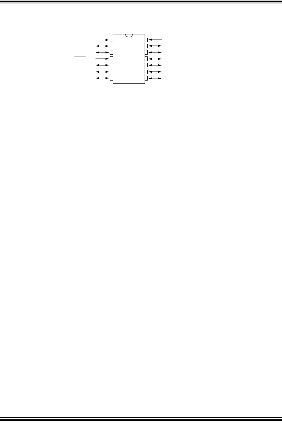
FIGURE 1: 14-PIN PDIP AND SOIC DIAGRAM
VDD
RB5/OSC1/CLKIN
RB4/OSC2/CLKOUT
RB3/MCLR
/VPP
RC5/T0CKI
RC4/C2OUT
RC3
VSS
RB0/C1IN+/AN0/ICSPDAT
RB1/C1IN-/AN1/ICSPCLK
RB2/C1OUT/AN2
RC0/C2IN+
RC1/C2IN-
RC2/CV
REF
MCV14A
1
2
3
4
5
6
7
8
9
10
11
12
13
14

© 2009 Microchip Technology Inc. Preliminary DS41338C-page 5
MCV14A
Table of Contents
1.0 General Description..................................................................................................................................................................... 7
2.0 Architectural Overview ................................................................................................................................................................ 9
3.0 Memory Organization................................................................................................................................................................ 13
4.0 Flash Data Memory................................................................................................................................................................... 21
5.0 I/O Port...................................................................................................................................................................................... 25
6.0 Timer0 Module and TMR0 Register .......................................................................................................................................... 29
7.0 Special Features of the CPU..................................................................................................................................................... 35
8.0 Analog-to-Digital (A/D) Converter.............................................................................................................................................. 49
9.0 Comparator(s)........................................................................................................................................................................... 53
10.0 Comparator Voltage Reference Module.................................................................................................................................... 59
11.0 Electrical Characteristics........................................................................................................................................................... 61
12.0 Packaging Information............................................................................................................................................................... 73
Index ................................................................................................................................................................................................... 79
Product Identification System ............................................................................................................................................................. 81
TO OUR VALUED CUSTOMERS
It is our intention to provide our valued customers with the best documentation possible to ensure successful use of your Micro-
chip products. To this end, we will continue to improve our publications to better suit your needs. Our publications will be refined
and enhanced as new volumes and updates are introduced.
If you have any questions or comments regarding this publication, please contact the Marketing Communications Department via
E-mail at [email protected] or fax the Reader Response Form in the back of this data sheet to (480) 792-4150.
We welcome your feedback.
Most Current Data Sheet
To obtain the most up-to-date version of this data sheet, please register at our Worldwide Web site at:
http://www.microchip.com
You can determine the version of a data sheet by examining its literature number found on the bottom outside corner of any page.
The last character of the literature number is the version number, (e.g., DS30000A is version A of document DS30000).
Errata
An errata sheet, describing minor operational differences from the data sheet and recommended workarounds, may exist for current
devices. As device/documentation issues become known to us, we will publish an errata sheet. The errata will specify the revision
of silicon and revision of document to which it applies.
To determine if an errata sheet exists for a particular device, please check with one of the following:
• Microchip’s Worldwide Web site; http://www.microchip.com
• Your local Microchip sales office (see last page)
• The Microchip Corporate Literature Center; U.S. FAX: (480) 792-7277
When contacting a sales office or the literature center, please specify which device, revision of silicon and data sheet (include lit-
erature number) you are using.
Customer Notification System
Register on our web site at www.microchip.com/cn to receive the most current information on all of our products.

MCV14A
DS41338C-page 6 Preliminary © 2009 Microchip Technology Inc.
NOTES:

© 2009 Microchip Technology Inc. Preliminary DS41338C-page 7
MCV14A
1.0 GENERAL DESCRIPTION
The MCV14A device from Microchip Technology is
low-cost, high-performance, 8-bit, fully-static, Flash-
based CMOS microcontrollers. It employs a RISC
architecture with only 33 single-word/single-cycle
instructions. All instructions are single cycle (200 μs)
except for program branches, which take two cycles.
The MCV14A device delivers performance an order of
magnitude higher than their competitors in the same
price category. The 12-bit wide instructions are highly
symmetrical, resulting in a typical 2:1 code compres-
sion over other 8-bit microcontrollers in its class. The
easy-to-use and easy to remember instruction set
reduces development time significantly.
The MCV14A product is equipped with special features
that reduce system cost and power requirements. The
Power-on Reset (POR) and Device Reset Timer (DRT)
eliminate the need for external Reset circuitry. There
are four oscillator configurations to choose from,
including INTRC Internal Oscillator mode and the
power-saving LP (Low-Power) Oscillator mode. Power-
Saving Sleep mode, Watchdog Timer and code protec-
tion features improve system cost, power and reliability.
The MCV14A device is available in the cost-effective
Flash programmable version, which is suitable for
production in any volume. The customer can take full
advantage of Microchip’s price leadership in Flash
programmable microcontrollers, while benefiting from
the Flash programmable flexibility.
The MCV14A product is supported by a full-featured
macro assembler, a software simulator, an in-circuit
emulator, a ‘C’ compiler, a low-cost development pro-
grammer and a full featured programmer. All the tools
are supported on PC and compatible machines.
1.1 Applications
The MCV14A device fits in applications ranging from
personal care appliances and security systems to low-
power remote transmitters/receivers. The Flash tech-
nology makes customizing application programs
(transmitter codes, appliance settings, receiver fre-
quencies, etc.) extremely fast and convenient. The
small footprint packages, for through hole or surface
mounting, make these microcontrollers perfect for
applications with space limitations. Low cost, low
power, high performance, ease of use and I/O flexibility
make the MCV14A device very versatile even in areas
where no microcontroller use has been considered
before (e.g., timer functions, logic and PLDs in larger
systems and coprocessor applications).
TABLE 1-1: FEATURES AND MEMORY OF MCV14A
MCV14A
Clock Maximum Frequency of Operation (MHz) 20
Memory Flash Program Memory 1024
SRAM Data Memory (bytes) 67
Flash Data Memory 64
Peripherals Timer Module(s) TMR0
Wake-up from Sleep on Pin Change Yes
Features I/O Pins 11
Input Pins 1
Internal Pull-ups Yes
In-Circuit Serial Programming™ Yes
Number of Instructions 33
Packages 14-pin PDIP and SOIC
The MCV14A device has Power-on Reset, selectable Watchdog Timer, selectable code-protect, high I/O current capability and
precision internal oscillator.
The MCV14A device uses serial programming with data pin RB0 and clock pin RB1.

MCV14A
DS41338C-page 8 Preliminary © 2009 Microchip Technology Inc.
NOTES:

© 2009 Microchip Technology Inc. Preliminary DS41338C-page 9
MCV14A
2.0 ARCHITECTURAL OVERVIEW
The high performance of the MCV14A device can be
attributed to a number of architectural features
commonly found in RISC microprocessors. To begin
with, the MCV14A device uses a Harvard architecture
in which program and data are accessed on separate
buses. This improves bandwidth over traditional von
Neumann architectures where program and data are
fetched on the same bus. Separating program and
data memory further allows instructions to be sized
differently than the 8-bit wide data word. Instruction
opcodes are 12 bits wide, making it possible to have
all single-word instructions. A 12-bit wide program
memory access bus fetches a 12-bit instruction in a
single cycle. A two-stage pipeline overlaps fetch and
execution of instructions. Consequently, all
instructions (33) execute in a single cycle (200 ns @
20 MHz, 1 μs @ 4 MHz) except for program
branches.
Table 2-1 below lists memory supported by the
MCV14A device.
TABLE 2-1: MCV14A MEMORY
The MCV14A device can directly or indirectly address
its register files and data memory. All Special Function
Registers (SFR), including the PC, are mapped in the
data memory. The MCV14A device has a highly orthog-
onal (symmetrical) instruction set that makes it possible
to carry out any operation, on any register, using any
Addressing mode. This symmetrical nature and lack of
“special optimal situations” make programming with the
MCV14A device simple, yet efficient. In addition, the
learning curve is reduced significantly.
The MCV14A device contains an 8-bit ALU and
working register. The ALU is a general purpose
arithmetic unit. It performs arithmetic and Boolean
functions between data in the working register and any
register file.
The ALU is 8 bits wide and capable of addition,
subtraction, shift and logical operations. Unless
otherwise mentioned, arithmetic operations are two’s
complement in nature. In two-operand instructions, one
operand is typically the W (working) register. The other
operand is either a file register or an immediate
constant. In single operand instructions, the operand is
either the W register or a file register.
The W register is an 8-bit working register used for ALU
operations. It is not an addressable register.
Depending on the instruction executed, the ALU may
affect the values of the Carry (C), Digit Carry (DC) and
Zero (Z) bits in the STATUS register. The C and DC bits
operate as a borrow
and digit borrow out bit, respec-
tively, in subtraction. See the SUBWF and ADDWF
instructions for examples.
A simplified block diagram is shown in Figure 2-2, with
the corresponding device pins described in Table 2-2.
Device
Program
Memory
Data Memory
Flash
(words)
SRAM
(bytes)
Flash
(bytes)
MCV14A 1024 67 64

MCV14A
DS41338C-page 10 Preliminary © 2009 Microchip Technology Inc.
FIGURE 2-1: MCV14A BLOCK DIAGRAM
11
Data Bus
8
12
Program
Bus
Instruction Reg
Program Counter
RAM
File
Registers
Direct Addr
5
RAM Addr
(1)
9
Addr MUX
Indirect
Addr
FSR Reg
STATUS Reg
MUX
ALU
W Reg
Device Reset
Power-on
Reset
Watchdog
Timer
Instruction
Decode and
Control
Timing
Generation
OSC1/CLKIN
OSC2/CLKOUT
MCLR
VDD, VSS
Timer0
PORTB
8
8
RB4/OSC2/CLKOUT
RB3/MCLR/VPP
RB2
RB1/ICSPCLK
RB0/ICSPDAT
5-7
3
RB5/OSC1/CLKIN
STACK1
STACK2
67
Internal RC
Clock
bytes
Timer
PORTC
RC4
RC3
RC2
RC1
RC0
RC5/T0CKI
Comparator 2
C1IN+
C1IN-
C1OUT
C2IN+
C2IN-
C2OUT
AN0
AN1
AN2
VREF
8-bit ADC
CVREF
CVREF
CVREF
VREF
Comparator 1
Flash Program
Memory
1K x 12
Memory
64x8
Flash Data

© 2009 Microchip Technology Inc. Preliminary DS41338C-page 11
MCV14A
TABLE 2-2: MCV14A PINOUT DESCRIPTION
Name Function
Input
Type
Output
Type
Description
RB0//C1IN+/AN0/
ICSPDAT
RB0 TTL CMOS Bidirectional I/O pin. Can be software programmed for internal
weak pull-up and wake-up from Sleep on pin change.
C1IN+ AN — Comparator 1 input.
AN0 AN — ADC channel input.
ICSPDAT ST CMOS ICSP™ mode Schmitt Trigger.
RB1/C1IN-/AN1/
ICSPCLK
RB1 TTL CMOS Bidirectional I/O pin. Can be software programmed for internal
weak pull-up and wake-up from Sleep on pin change.
C1IN- AN — Comparator 1 input.
AN1 AN — ADC channel input.
ICSPCLK ST CMOS ICSP mode Schmitt Trigger.
RB2/C1OUT/AN2 RB2 TTL CMOS Bidirectional I/O pin.
C1OUT — CMOS Comparator 1 output.
AN2 AN — ADC channel input.
RB3/MCLR
/VPP RB3 TTL — Input pin. Can be software programmed for internal weak
pull-up and wake-up from Sleep on pin change.
MCLR ST — Master Clear (Reset). When configured as MCLR, this pin is
an active-low Reset to the device. Voltage on MCLR
/VPP must
not exceed V
DD during normal device operation or the device
will enter Programming mode. Weak pull-up always on if
configured as MCLR.
VPP HV — Programming voltage input.
RB4/OSC2/CLKOUT RB4 TTL CMOS Bidirectional I/O pin.
OSC2 — XTAL Oscillator crystal output. Connections to crystal or resonator in
Crystal Oscillator mode (XT, HS and LP modes only, PORTB
in other modes).
CLKOUT — CMOS EXTRC/INTRC CLKOUT pin (F
OSC/4).
RB5/OSC1/CLKIN RB5 TTL CMOS Bidirectional I/O pin.
OSC1 XTAL — Oscillator crystal input.
CLKIN ST — External clock source input.
RC0/C2IN+ RC0 TTL CMOS Bidirectional I/O port.
C2IN+ AN — Comparator 2 input.
RC1/C2IN- RC1 TTL CMOS Bidirectional I/O port.
C2IN- AN — Comparator 2 input.
RC2/CV
REF RC2 TTL CMOS Bidirectional I/O port.
CVREF — AN Programmable Voltage Reference output.
RC3 RC3 TTL CMOS Bidirectional I/O port.
RC4/C2OUT RC4 TTL CMOS Bidirectional I/O port.
C2OUT — CMOS Comparator 2 output.
RC5/T0CKI RC5 TTL CMOS Bidirectional I/O port.
T0CKI ST — Timer0 Schmitt Trigger input pin.
V
DD VDD — P Positive supply for logic and I/O pins.
V
SS VSS — P Ground reference for logic and I/O pins.
Legend: I = Input, O = Output, I/O = Input/Output, P = Power, — = Not used, TTL = TTL input,
ST = Schmitt Trigger input, HV = High Voltage

MCV14A
DS41338C-page 12 Preliminary © 2009 Microchip Technology Inc.
2.1 Clocking Scheme/Instruction
Cycle
The clock input (OSC1/CLKIN pin) is internally divided
by four to generate four non-overlapping quadrature
clocks, namely Q1, Q2, Q3 and Q4. Internally, the PC
is incremented every Q1 and the instruction is fetched
from program memory and latched into the instruction
register in Q4. It is decoded and executed during the
following Q1 through Q4. The clocks and instruction
execution flow is shown in Figure 2-2 and Example 2-1.
2.2 Instruction Flow/Pipelining
An instruction cycle consists of four Q cycles (Q1, Q2,
Q3 and Q4). The instruction fetch and execute are
pipelined such that fetch takes one instruction cycle,
while decode and execute take another instruction
cycle. However, due to the pipelining, each instruction
effectively executes in one cycle. If an instruction
causes the PC to change (e.g., GOTO), then two cycles
are required to complete the instruction (Example 2-1).
A fetch cycle begins with the PC incrementing in Q1.
In the execution cycle, the fetched instruction is latched
into the Instruction Register (IR) in cycle Q1. This
instruction is then decoded and executed during the
Q2, Q3 and Q4 cycles. Data memory is read during Q2
(operand read) and written during Q4 (destination
write).
FIGURE 2-2: CLOCK/INSTRUCTION CYCLE
EXAMPLE 2-1: INSTRUCTION PIPELINE FLOW
Q1
Q2 Q3 Q4
Q1
Q2 Q3 Q4
Q1
Q2 Q3 Q4
OSC1
Q1
Q2
Q3
Q4
PC
PC
PC + 1 PC + 2
Fetch INST (PC)
Execute INST (PC – 1)
Fetch INST (PC + 1)
Execute INST (PC)
Fetch INST (PC + 2)
Execute INST (PC + 1)
Internal
Phase
Clock
All instructions are single cycle, except for any program branches. These take two cycles, since the fetch instruction
is “flushed” from the pipeline, while the new instruction is being fetched and then executed.
1. MOVLW 03H
Fetch 1 Execute 1
2. MOVWF PORTB
Fetch 2 Execute 2
3. CALL SUB_1
Fetch 3 Execute 3
4. BSF PORTB, BIT1
Fetch 4 Flush
Fetch SUB_1 Execute SUB_1

© 2009 Microchip Technology Inc. Preliminary DS41338C-page 13
MCV14A
3.0 MEMORY ORGANIZATION
The MCV14A memories are organized into program
memory and data memory (SRAM).The self-writable
portion of the program memory called Flash data mem-
ory is located at addresses at 400h-43Fh. All Program
mode commands that work on the normal Flash mem-
ory work on the Flash data memory. This includes bulk
erase, row/column/cycling toggles, Load and Read
data commands (Refer to Section 4.0 “Flash Data
Memory” for more details). For devices with more than
512 bytes of program memory, a paging scheme is
used. Program memory pages are accessed using one
STATUS register bit. For the MCV14A, with data mem-
ory register files of more than 32 registers, a banking
scheme is used. Data memory banks are accessed
using the File Select Register (FSR).
3.1 Program Memory Organization for
the MCV14A
The MCV14A device has an 11-bit Program Counter
(PC) capable of addressing a 2K x 12 program memory
space. Program memory is partitioned into user memory,
data memory and configuration memory spaces.
The user memory space is the on-chip user program
memory. As shown in Figure 3-1, it extends from 0x000
to 0x3FF and partitions into pages, including Reset
vector at address 0x3FF.
The data memory space is the Flash data memory
block and is located at addresses PC = 400h-43Fh. All
Program mode commands that work on the normal
Flash memory work on the Flash data memory block.
This includes bulk erase, Load and Read data
commands.
The Configuration Memory Space extends from 0x440
to 0x7FF. Locations from 0x448 through 0x49F are
reserved. The User I.D. locations extend from 0x440
through 0x443. The Backup OSCCAL locations extend
from 0x444 through 0x447. The Configuration Word is
physically located at 0x7FF.
FIGURE 3-1: MEMORY MAP
000h
1FFh
Reset Vector
On-chip User
Program
Memory (Page 0)
200h
3FFh
3FEh
User ID Locations
Reserved
Configuration Word
400h
443h
444h
7FEh
7FFh
43Fh
440h
Unimplemented
On-chip User
Program
Memory (Page 1)
Data Memory
Flash Data Memory
448h
49Fh
Backup OSCCAL
Locations
447h
4A0h
Configuration Memory
Space
Space
User Memory
Space

MCV14A
DS41338C-page 14 Preliminary © 2009 Microchip Technology Inc.
3.2 Data Memory (SRAM and FSRs)
Data memory is composed of registers or bytes of
SRAM. Therefore, data memory for a device is
specified by its register file. The register file is divided
into two functional groups: Special Function Registers
(SFR) and General Purpose Registers (GPR).
The Special Function Registers are registers used by
the CPU and peripheral functions for controlling
desired operations of the MCV14A. See Figure 3-2 for
details.
The MCV14A register file is composed of 13 Special
Function Registers and 41 General Purpose Registers
3.2.1 GENERAL PURPOSE REGISTER
FILE
The General Purpose Register file is accessed, either
directly or indirectly, through the File Select Register
(FSR). See Section 3.8 “Indirect Data Addressing:
INDF and FSR Registers”.
3.2.2 SPECIAL FUNCTION REGISTERS
The Special Function Registers (SFRs) are registers
used by the CPU and peripheral functions to control the
operation of the device (Table 3-1).
The Special Function Registers can be classified into
two sets. The Special Function Registers associated
with the “core” functions are described in this section.
Those related to the operation of the peripheral
features are described in the section for each
peripheral feature.
FIGURE 3-2: REGISTER FILE MAP
File Address
00h
01h
02h
03h
04h
05h
06h
07h
1Fh
INDF
(1)
TMR0
PCL
STATUS
FSR
OSCCAL
PORTB
10h
Bank 0 Bank 1 Bank 2 Bank 3
3Fh
30h
20h
5Fh
50h
40h
7Fh
70h
60h
General
Purpose
Registers
General
Purpose
Registers
General
Purpose
Registers
General
Purpose
Registers
General
Purpose
Registers
PORTC
08h
Note 1: Not a physical register. See Section 3.8 “Indirect Data Addressing: INDF and FSR Registers”.
FSR<6:5> 00 01 10 11
2Fh 4Fh 6Fh
0Dh
CM1CON0
CM2CON0
VRCON
09h
0Ah
0Bh
ADRES
ADCON0
0Ch
0Fh
INDF
(1)
EECON
PCL
STATUS
FSR
EEDATA
EEADR
CM1CON0
CM2CON0
VRCON
ADRES
ADCON0
INDF
(1)
TMR0
PCL
STATUS
FSR
OSCCAL
PORTB
PORTC
VRCON
ADRES
ADCON0
INDF
(1)
EECON
PCL
STATUS
FSR
EEDATA
EEADR
VRCON
ADRES
ADCON0
CM1CON0
CM1CON0
CM2CON0
CM2CON0
PORTC
PORTC
Addresses map back to
addresses in Bank 0.

© 2009 Microchip Technology Inc. Preliminary DS41338C-page 15
MCV14A
3.2.3 SPECIAL FUNCTION REGISTERS
The Special Function Registers (SFRs) are registers
used by the CPU and peripheral functions to control the
operation of the device (Table 3-1).
The Special Function Registers can be classified into
two sets. The Special Function Registers associated
with the “core” functions are described in this section.
Those related to the operation of the peripheral
features are described in the section for each
peripheral feature.
TABLE 3-1: SPECIAL FUNCTION REGISTER (SFR) SUMMARY
Addr Name Bit 7 Bit 6 Bit 5 Bit 4 Bit 3 Bit 2 Bit 1 Bit 0
Value on
Power-on
Reset
Page
#
N/A TRIS
— — I/O Control Register (PORTB, PORTC) --11 1111 25
N/A OPTION Contains control bits to configure Timer0 and Timer0/WDT prescaler 1111 1111 17
00h INDF Uses contents of FSR to Address Data Memory (not a physical register) xxxx xxxx 20
01h/41h TMR0 Timer0 Module Register xxxx xxxx 29
02h
(1)
PCL Low order 8 bits of PC 1111 1111 19
03h STATUS RBWUF CWUF PA0 TO
PD ZDCC0001 1xxx 16
04h FSR Indirect Data Memory Address Pointer 100x xxxx 20
05h/45h OSCCAL CAL6 CAL5 CAL4 CAL3 CAL2 CAL1 CAL0
— 1111 111- 18
06h/46h PORTB
— — RB5 RB4 RB3 RB2 RB1 RB0 --xx xxxx 25
07h PORTC
— — RC5 RC4 RC3 RC2 RC1 RC0 --xx xxxx 26
08h CM1CON0 C1OUT C1OUTEN
C1POL C1T0CS C1ON C1NREF C1PREF C1WU 1111 1111 53
09h ADCON0 ANS1 ANS0 ADCS1 ADCS0 CHS1 CHS0 GO/DONE
ADON 1111 1100 51
0Ah ADRES ADC Conversion Result xxxx xxxx 52
0Bh CM2CON0 C2OUT C2OUTEN
C2POL C2PREF2 C2ON C2NREF C2PREF1 C2WU 1111 1111 54
0Ch VRCON VREN VROE VRR
— VR3 VR2 VR1 VR0 000- 0000 59
21h/61h EECON
— — — FREE WRERR WREN WR RD ---0 0000 22
25h/65h EEDATA SELF READ/WRITE DATA xxxx xxxx 21
26h/66h EEADR
— — SELF READ/WRITE ADDRESS --xx xxxx 21
Legend: x = unknown, u = unchanged, – = unimplemented, read as '0' (if applicable). Shaded cells = unimplemented or unused
Note 1: The upper byte of the Program Counter is not directly accessible. See Section 3.6 “Program Counter” for an explanation of how to
access these bits.

MCV14A
DS41338C-page 16 Preliminary © 2009 Microchip Technology Inc.
3.3 STATUS Register
This register contains the arithmetic status of the ALU,
the Reset status and the page preselect bit.
The STATUS register can be the destination for any
instruction, as with any other register. If the STATUS
register is the destination for an instruction that affects
the Z, DC or C bits, then the write to these three bits is
disabled. These bits are set or cleared according to the
device logic. Furthermore, the TO
and PD bits are not
writable. Therefore, the result of an instruction with the
STATUS register as destination may be different than
intended.
For example, CLRF STATUS, will clear the upper three
bits and set the Z bit. This leaves the STATUS register
as 000u u1uu (where u = unchanged).
Therefore, it is recommended that only BCF, BSF and
MOVWF instructions be used to alter the STATUS
register. These instructions do not affect the Z, DC or C
bits from the STATUS register.
REGISTER 3-1: STATUS: STATUS REGISTER
R/W-0 R/W-0 R/W-0 R-1 R-1 R/W-x R/W-x R/W-x
RBWUF CWUF PA0 TO PD ZDCC
bit 7 bit 0
Legend:
R = Readable bit W = Writable bit U = Unimplemented bit, read as ‘0’
-n = Value at POR ‘1’ = Bit is set ‘0’ = Bit is cleared x = Bit is unknown
bit 7 RBWUF: Wake-up from Sleep on Pin Change bit
1 = Reset due to wake-up from Sleep on pin change
0 = After power-up or other Reset
bit 6 CWUF: Wake-up from Sleep on Comparator Change bit
1 = Reset due to wake-up from Sleep on comparator change
0 = After power-up or other Reset
bit 5 PA0: Program Page Preselect bit
1 = Page 1 (000h-1FFh)
0 = Page 0 (200h-3FFh)
bit 4 TO
: Time-out bit
1 = After power-up, CLRWDT instruction, or SLEEP instruction
0 = A WDT time-out occurred
bit 3 PD
: Power-down bit
1 = After power-up or by the CLRWDT instruction
0 = By execution of the SLEEP instruction
bit 2 Z: Zero bit
1 = The result of an arithmetic or logic operation is zero
0 = The result of an arithmetic or logic operation is not zero
bit 1 DC: Digit carry/borrow
bit (for ADDWF and SUBWF instructions)
ADDWF:
1 = A carry from the 4th low-order bit of the result occurred
0 = A carry from the 4th low-order bit of the result did not occur
SUBWF:
1 = A borrow from the 4th low-order bit of the result did not occur
0 = A borrow from the 4th low-order bit of the result occurred
bit 0 C: Carry/borrow bit (for ADDWF, SUBWF and RRF, RLF instructions)
ADDWF: SUBWF: RRF or RLF:
1 = A carry occurred 1 = A borrow did not occur Load bit with LSb or MSb, respectively
0 = A carry did not occur 0 = A borrow occurred

© 2009 Microchip Technology Inc. Preliminary DS41338C-page 17
MCV14A
3.4 OPTION Register
The OPTION register is a 8-bit wide, write-only register,
which contains various control bits to configure the
Timer0/WDT prescaler and Timer0.
By executing the OPTION instruction, the contents of
the W register will be transferred to the OPTION
register. A Reset sets the OPTION<7:0> bits.
Note: If TRIS bit is set to ‘0’, the wake-up on
change and pull-up functions are disabled
for that pin (i.e., note that TRIS overrides
Option control of RBPU
and RBWU).
REGISTER 3-2: OPTION: OPTION REGISTER
W-1 W-1 W-1 W-1 W-1 W-1 W-1 W-1
RBWU
RBPU T0CS
(1)
T0SE PSA PS2 PS1 PS0
bit 7 bit 0
Legend:
R = Readable bit W = Writable bit U = Unimplemented bit, read as ‘0’
-n = Value at POR ‘1’ = Bit is set ‘0’ = Bit is cleared x = Bit is unknown
bit 7 RBWU
: Enable Wake-up On Pin Change bit
1 = Disabled
0 = Enabled
bit 6 RBPU
: Enable Weak Pull-ups bit
1 = Disabled
0 = Enabled
bit 5 T0CS: Timer0 Clock Source Select bit
(1)
1 = Transition on T0CKI pin
0 = Internal instruction cycle clock (CLKOUT)
bit 4 T0SE: Timer0 Source Edge Select bit
1 = Increment on high-to-low transition on T0CKI pin
0 = Increment on low-to-high transition on T0CKI pin
bit 3 PSA: Prescaler Assignment bit
1 = Prescaler assigned to the WDT
0 = Prescaler assigned to Timer0
bit 2-0 PS<2:0>: Prescaler Rate Select bits
Note 1: If the T0CS bit is set to ‘1’, it will override the TRIS function on the T0CKI pin.
000
001
010
011
100
101
110
111
1 : 2
1 : 4
1 : 8
1 : 16
1 : 32
1 : 64
1 : 128
1 : 256
1 : 1
1 : 2
1 : 4
1 : 8
1 : 16
1 : 32
1 : 64
1 : 128
Bit Value Timer0 Rate WDT Rate

MCV14A
DS41338C-page 18 Preliminary © 2009 Microchip Technology Inc.
3.5 OSCCAL Register
The Oscillator Calibration (OSCCAL) register is used
to calibrate the 8 MHz internal oscillator macro. It
contains 7 bits of calibration that uses a two’s
complement scheme for controlling the oscillator speed.
See Register 3-3 for details.
REGISTER 3-3: OSCCAL: OSCILLATOR CALIBRATION REGISTER
R/W-1 R/W-1 R/W-1 R/W-1 R/W-1 R/W-1 R/W-1 U-0
CAL6 CAL5 CAL4 CAL3 CAL2 CAL1 CAL0 —
bit 7 bit 0
Legend:
R = Readable bit W = Writable bit U = Unimplemented bit, read as ‘0’
-n = Value at POR ‘1’ = Bit is set ‘0’ = Bit is cleared x = Bit is unknown
bit 7-1 CAL<6:0>: Oscillator Calibration bits
0111111 = Maximum frequency
•
•
•
0000001
0000000 = Center frequency
1111111
•
•
•
1000000 = Minimum frequency
bit 0 Unimplemented: Read as ‘0’
© 2009 Microchip Technology Inc. Preliminary DS41338C-page 19
MCV14A
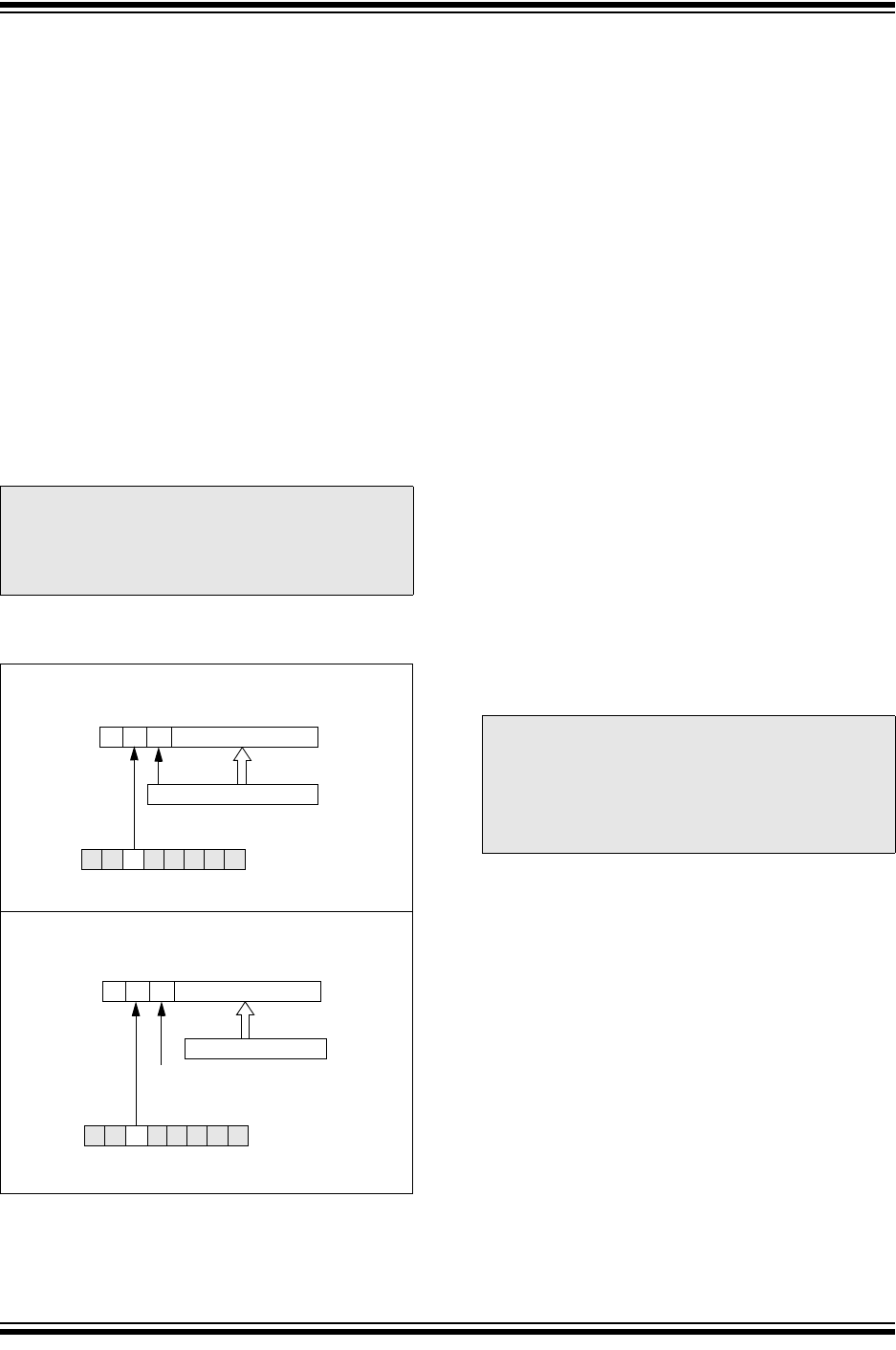
3.6 Program Counter
As a program instruction is executed, the Program
Counter (PC) will contain the address of the next
program instruction to be executed. The PC value is
increased by one every instruction cycle, unless an
instruction changes the PC.
For a GOTO instruction, bits 8:0 of the PC are provided
by the GOTO instruction word. The Program Counter
(PCL) is mapped to PC<7:0>. Bit 5 of the STATUS
register provides page information to bit 9 of the PC
(Figure 3-3).
For a CALL instruction, or any instruction where the
PCL is the destination, bits 7:0 of the PC again are
provided by the instruction word. However, PC<8>
does not come from the instruction word, but is always
cleared (Figure 3-3).
Instructions where the PCL is the destination, or modify
PCL instructions, include MOVWF PC, ADDWF PC and
BSF PC,5.
FIGURE 3-3: LOADING OF PC
BRANCH INSTRUCTIONS
3.6.1 EFFECTS OF RESET
The PC is set upon a Reset, which means that the PC
addresses the last location in the last page (i.e., the
oscillator calibration instruction). After executing
MOVLW XX, the PC will roll over to location 00h and
begin executing user code.
The STATUS register page preselect bits are cleared
upon a Reset, which means that page 0 is pre-selected.
Therefore, upon a Reset, a GOTO instruction will
automatically cause the program to jump to page 0 until
the value of the page bits is altered.
3.7 Stack
The MCV14A device has a 2-deep, 12-bit wide
hardware PUSH/POP stack.
A CALL instruction will PUSH the current value of Stack
1 into Stack 2 and then PUSH the current PC value,
incremented by one, into Stack Level 1. If more than two
sequential CALLs are executed, only the most recent two
return addresses are stored.
A RETLW instruction will POP the contents of Stack
Level 1 into the PC and then copy Stack Level 2
contents into Stack Level 1. If more than two sequential
RETLWs are executed, the stack will be filled with the
address previously stored in Stack Level 2. Note that
the W register will be loaded with the literal value
specified in the instruction. This is particularly useful for
the implementation of data look-up tables within the
program memory.
Note: Because PC<8> is cleared in the CALL
instruction or any modify PCL instruction,
all subroutine calls or computed jumps are
limited to the first 256 locations of any
program memory page (512 words long).
PA0
Status
PC
87 0
PCL
910
Instruction Word
7 0
GOTO Instruction
CALL or Modify PCL Instruction
PA0
Status
PC
87 0
PCL
910
Instruction Word
7 0
Reset to ‘0’
Note 1: There are no Status bits to indicate Stack
Overflows or Stack Underflow conditions.
2: There are no instruction mnemonics
called PUSH or POP. These are actions
that occur from the execution of the CALL
and RETLW instructions.
MCV14A
DS41338C-page 20 Preliminary © 2009 Microchip Technology Inc.
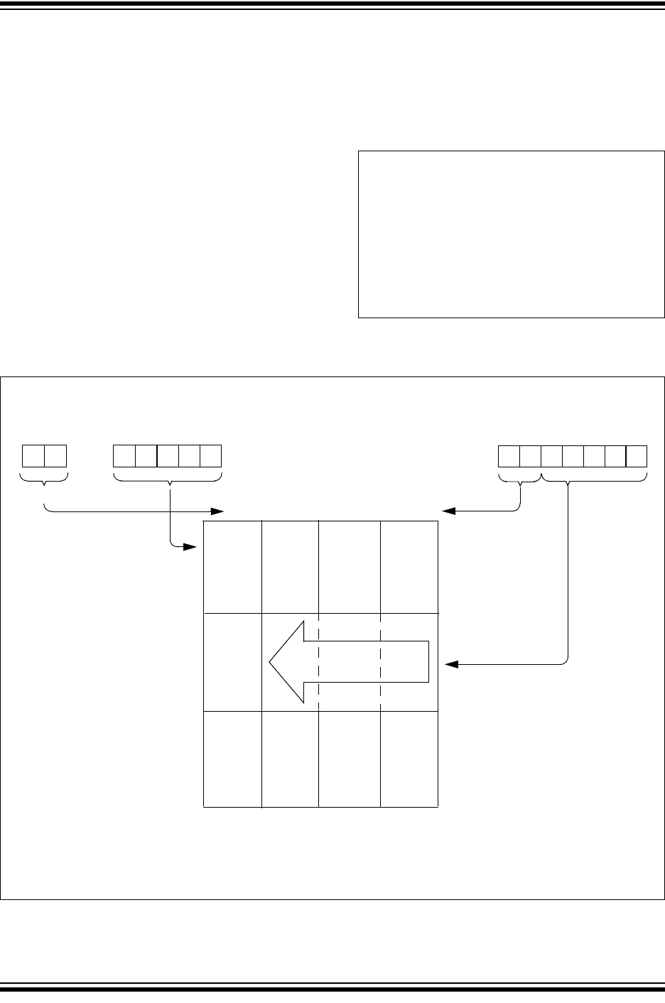
3.8 Indirect Data Addressing: INDF
and FSR Registers
The INDF Register is not a physical register.
Addressing INDF actually addresses the register
whose address is contained in the FSR Register (FSR
is a pointer). This is indirect addressing.
Reading INDF itself indirectly (FSR = 0) will produce
00h. Writing to the INDF Register indirectly results in a
no-operation (although Status bits may be affected).
The FSR is 8-bit wide register. It is used in conjunction
with the INDF Register to indirectly address the data
memory area.
The FSR<4:0> bits are used to select data memory
addresses 00h to 1Fh.
FSR<6:5> are the bank select bits and are used to
select the bank to be addressed (00 = Bank 0,
01 =Bank 1, 10 = Bank 2, 11 = Bank 3).
FSR<7> is unimplemented and read as ‘1’.
A simple program to clear RAM locations 10h-1Fh
using indirect addressing is shown in Example 3-1.
EXAMPLE 3-1: HOW TO CLEAR RAM
USING INDIRECT
ADDRESSING
FIGURE 3-4: DIRECT/INDIRECT ADDRESSING
MOVLW 0x10 ;initialize pointer
MOVWF FSR ;to RAM
NEXT CLRF INDF ;clear INDF
;register
INCF FSR,F ;inc pointer
BTFSC FSR,4 ;all done?
GOTO NEXT ;NO, clear next
CONTINUE
: ;YES, continue
:
Note 1: For register map detail see Figure 3-2.
bank
select
location select
location select
bank select
Indirect Addressing
Direct Addressing
Data
Memory
(1)
0Ch
0Dh
0
4
5
6
(FSR)
1000 01 11
00h
0Fh 2Fh 4Fh 6Fh
(opcode)
04
5
6
(FSR)
Addresses map back to
addresses in Bank 0.
3
2
1
3
2
1
10h
Bank 0 Bank 1 Bank 2 Bank 3
1Fh 3Fh 5Fh 7Fh

© 2009 Microchip Technology Inc. Preliminary DS41338C-page 21
MCV14A
4.0 FLASH DATA MEMORY
The data memory is the Flash data memory block,
which attaches to the user Flash program memory. It is
located at addresses 0x400-0x43F, as shown in Figure
5-1.
This Flash data memory block consists of 8 rows and
has self-write capability of up to 64 bytes. This memory
block is not directly mapped in the register file space.
Instead, it is indirectly addressed through the Special
Function Registers. There are three SFRs used to read
and write this memory:
• EEDATA (Register 4-1)
• EEADR (Register 4-2)
• EECON (Register 4-3)
EEDATA holds the 8-bit data for read/write, and
EEADR holds the address of the EEDATA location
being accessed. The effective program counter is
EEADR + 400h with only the lower 8 bits of each word
being readable or writable.
• EEADR = 00h, PC = 400h
• EEADR = 01h, PC = 401h
The Flash data memory allows byte read and write, and
during the operations of read and write cycles, the CPU
stalls.
The timing for all self-writes and erases is controlled by
the internal timing block of the program memory (see
Section 11.0 “Electrical Characteristics”,
Table 11-11). The write/erase voltages are generated
by an on-chip charge pump rated to operate over the
voltage range of the device for byte or word operations.
When the device is code-protected, the CPU may
continue to read and write the Flash data memory and
read the program memory. When code-protected, the
device programmer can no longer access data or
program memory.
REGISTER 4-1: EEDATA: FLASH DATA REGISTER
R/W-x R/W-x R/W-x R/W-x R/W-x R/W-x R/W-x R/W-x
EEDATA7 EEDATA6 EEDATA5 EEDATA4 EEDATA3 EEDATA2 EEDATA1 EEDATA0
bit 7 bit 0
Legend:
R = Readable bit W = Writable bit U = Unimplemented bit, read as ‘0’
-n = Value at POR ‘1’ = Bit is set ‘0’ = Bit is cleared x = Bit is unknown
bit 7-0 EEDATA<7:0>: 8-bits of data to be read from/written to data Flash
REGISTER 4-2: EEADR: FLASH ADDRESS REGISTER
U-0 U-0 R/W-x R/W-x R/W-x R/W-x R/W-x R/W-x
— — EEADR5 EEADR4 EEADR3 EEADR2 EEADR1 EEADR0
bit 7 bit 0
Legend:
R = Readable bit W = Writable bit U = Unimplemented bit, read as ‘0’
-n = Value at POR ‘1’ = Bit is set ‘0’ = Bit is cleared x = Bit is unknown
bit 7-6 Unimplemented: Do not use
bit 5-0 EEADR<5:0>: 6-bits of data to be read from/written to data Flash

MCV14A
DS41338C-page 22 Preliminary © 2009 Microchip Technology Inc.
REGISTER 4-3: EECON: FLASH CONTROL REGISTER
U-0 U-0 U-0 R/W-0 R/W-0 R/W-0 R/W-0
R/W-0
— — — FREE WRERR WREN WR
RD
bit 7
bit 0
Legend:
S = Bit can only be set
R = Readable bit W = Writable bit U = Unimplemented bit, read as ‘0’
-n = Value at POR ‘1’ = Bit is set ‘0’ = Bit is cleared x = Bit is unknown
bit 7-5 Unimplemented: Do not use
bit 4 FREE: Flash Data Memory Row Erase Enable Bit
1 = Program memory row being pointed to by EEADR will be erased on the next write cycle. No write
will be performed. This bit is cleared at the completion of the erase operation.
0 = Perform write only
bit 3 WRERR: Write Error Flag bit
1 = A write operation terminated prematurely (by device Reset)
0 = Write operation completed successfully
bit 2 WREN: Write Enable bit
1 = Allows write cycle to Flash data memory
0 = Inhibits write cycle to Flash data memory
bit 1 WR: Write Control bit
1 = Initiate a erase or write cycle
0 = Write/Erase cycle is complete
bit 0 RD: Read Control bit
1 = Initiate a read of Flash data memory
0 = Do not read Flash data memory

© 2009 Microchip Technology Inc. Preliminary DS41338C-page 23
MCV14A
4.1 Reading Data Memory
To read a memory location, the user must write the
address to be read into the EEADR register and then
set the RD bit in the EECON register. The data will be
available in the next instruction cycle.
EXAMPLE 4-1: FLASH DATA MEMORY
READ
4.2 Erasing a Data Memory Row
In order to write new data to the Flash data memory,
the program memory row that is being addressed by
EEADR<5:0> must be erased.
To prevent a spurious row erasure, a specific
sequence must be executed to initiate the erase to the
program memory. The sequence is as follows:
- Set the FREE bit (enable Flash data memory
row erase)
- Set the WREN bit (enable writes to the Flash
data memory array)
- Set the WR bit (initiates the row erase of the
Flash data memory array)
If the WREN bit is not set in the instruction cycle after
the FREE bit is set, the FREE bit will be cleared in
hardware.
If the WR bit is not set in the instruction cycle after the
WREN bit is set, the WREN bit will be cleared in
hardware.
Both of these sequences is to prevent an accidental
erase of the Flash data memory.
EXAMPLE 4-2: ERASE DATA MEMORY
ROW
4.3 Writing a Data Memory Word
To write a memory location, the user must write the
address to be written to into the EEADR register. He
must then load the data to be written into the EEDATA
register. Once the data and address have been
loaded, a specific sequence must be executed to
initiate the write to the program memory. The
sequence is as follows:
• Set the WREN bit (enable writes to the Flash data
memory array)
• Set the WR bit (initiates the write to the Flash data
memory array)
If the WR bit is not set in the instruction cycle after the
WREN bit is set, the WREN bit will be cleared in
hardware.
This sequence is to prevent an accidental write to the
Flash memory.
Note: Only a BSF command will work to enable the
Flash data memory read documented in
Example 4-1. No other sequence of com-
mands will work, no exceptions.
BSF FSR,5 ;SWITCH TO BANK 1
MOVLW EE_ADR_READ ;LOAD ADDRESS TO READ
BSF EECON,RD ;INITITATE THE READ
INSTRUCTION
;IS DECODED
MOVF EEDATA,W ;GET NEW DATA
Note: The FREE bit may be set by any command
normally used by the core. However, the
WREN and WR bits can only be set using a
series of BSF commands, as documented in
Example 4-2. No other sequence of
commands will work, no exceptions.
BSF FSR,5 ;SWITCH TO BANK 1
MOVLW EE_ADR_ERASE ;LOAD ADDRESS TO ERASE
MOVWF EEADR ;LOAD ADDRESS TO SFR
BSF EECON,FREE ;SELECT ERASE
BSF EECON,WREN ;ENABL FLASH PROG’ING
BSF EECON,WR ;INITITATE ERASE
xxx ;NEXT INSTRUCTION

MCV14A
DS41338C-page 24 Preliminary © 2009 Microchip Technology Inc.
EXAMPLE 4-3: DATA MEMORY WRITE
4.4 DATA MEMORY OPERATION
DURING CODE-PROTECT
Data memory can be code-protected by programming
the CPDF
bit in the Configuration Word (Register 7-1)
to ‘0’.
Note 1: Only a series of BSF commands will work
to enable the memory write sequence
documented in Example 4-3. No other
sequence of commands will work, no
exceptions.
2: For reads, erases and writes to the Flash
data memory, there is no need to insert a
NOP into the user code as is done on
mid-range devices. The instruction imme-
diately following the “BSF EECON,WR/RD”
will be fetched and executed properly.
BSF FSR,5 ;SWITCH TO BANK 1
MOVLW EE_ADR_WRITE ;LOAD ADDRESS TO
;WRITE
MOVWF EEADR ;INTO EEADR
;REGISTER
MOVLW EE_DATA_TO_WRITE;LOAD DATA TO
MOVWF EEDATA ;INTO EEDATA
;REGISTER
BSF EECON,WREN ;ENABLE WRITES
BSF EECON,WR ;START WRITE
;SEQUENCE
NOP ;WAIT AS READ
;INSTRUCTION
;IS DECODED
NOP ;INSTRUCTION
IGNORED

© 2009 Microchip Technology Inc. Preliminary DS41338C-page 25
MCV14A
5.0 I/O PORT
As with any other register, the I/O register(s) can be
written and read under program control. However, read
instructions (e.g., MOVF PORTB,W) always read the I/O
pins independent of the pin’s Input/Output modes. On
Reset, all I/O ports are defined as input (inputs are at high-
impedance) since the I/O control registers are all set.
5.1 PORTB
PORTB is a 6-bit I/O register. Only the low-order 6 bits
are used (RB<5:0>). Bits 7 and 6 are unimplemented
and read as ‘0’s. Please note that RB3 is an input only
pin. The Configuration Word can set several I/O’s to
alternate functions. When acting as alternate functions,
the pins will read as ‘0’ during a port read. Pins RB0,
RB1, RB3 and RB4 can be configured with weak pull-
ups and also for wake-up on change. The wake-up on
change and weak pull-up functions are not pin select-
able. If RB3/MCLR
is configured as MCLR, weak pull-
up is always on and wake-up on change for this pin is
not enabled.
5.2 PORTC
PORTC is a 6-bit I/O register. Only the low-order 6 bits
are used (RC<5:0>). Bits 7 and 6 are unimplemented
and read as ‘0’s.
5.3 TRIS Register
The Output Driver Control register is loaded with the
contents of the W register by executing the TRIS f
instruction. A ‘1’ from a TRIS register bit puts the corre-
sponding output driver in a High-Impedance mode. A
‘0’ puts the contents of the output data latch on the
selected pins, enabling the output buffer. The excep-
tions are RB3, which is input only and the T0CKI pin,
which may be controlled by the OPTION register. See
Register 3-2 and Register 3-3.
The TRIS register is “write-only” and is set (output
drivers disabled) upon Reset.
TABLE 5-1: WEAK PULL-UP ENABLED PINS
Device RB0 Weak Pull-up RB1 Weak Pull-up RB3 Weak Pull-up
(1)
RB4 Weak Pull-up
MCV14A Yes Yes Yes Yes
Note1: When MCLREN = 1, the weak pull-up on RB3/MCLR
is always enabled.
REGISTER 5-1: PORTB: PORTB REGISTER
U-0 U-0 R/W-x R/W-x R/W-x R/W-x R/W-x R/W-x
— — RB5 RB4 RB3 RB2 RB1 RB0
bit 7 bit 0
Legend:
R = Readable bit W = Writable bit U = Unimplemented bit, read as ‘0’
-n = Value at POR ‘1’ = Bit is set ‘0’ = Bit is cleared x = Bit is unknown
bit 7-6 Unimplemented: Read as ‘1’
bit 5-0 RB<5:0>: PORTB I/O Pin bits
1 = Port pin is >V
IH min.
0 = Port pin is <V
IL max.

MCV14A
DS41338C-page 26 Preliminary © 2009 Microchip Technology Inc.
REGISTER 5-2: PORTC: PORTC REGISTER
U-0 U-0 R/W-x R/W-x R/W-x R/W-x R/W-x R/W-x
— — RC5 RC4 RC3 RC2 RC1 RC0
bit 7 bit 0
Legend:
R = Readable bit W = Writable bit U = Unimplemented bit, read as ‘0’
-n = Value at POR ‘1’ = Bit is set ‘0’ = Bit is cleared x = Bit is unknown
bit 7-6 Unimplemented: Read as ‘1’
bit 5-0 RC<5:0>: PORTC I/O Pin bits
1 = Port pin is >V
IH min.
0 = Port pin is <V
IL max.

© 2009 Microchip Technology Inc. Preliminary DS41338C-page 27
MCV14A
5.4 I/O Interfacing
The equivalent circuit for an I/O port pin is shown in
Figure 5-1. All port pins, except RB3 which is input only,
may be used for both input and output operations. For
input operations, these ports are non-latching. Any
input must be present until read by an input instruction
(e.g., MOVF PORTB, W). The outputs are latched and
remain unchanged until the output latch is rewritten. To
use a port pin as output, the corresponding direction
control bit in TRIS must be cleared (= 0). For use as an
input, the corresponding TRIS bit must be set. Any I/O
pin (except RB3) can be programmed individually as
input or output.
FIGURE 5-1: MCV14A EQUIVALENT
CIRCUIT FOR A SINGLE
I/O PIN
TABLE 5-2: SUMMARY OF PORT REGISTERS
TABLE 5-3: I/O PINS ORDER OF PRECEDENCE
Data
Bus
Q
D
Q
CK
Q
D
Q
CK
P
N
WR
Port
TRIS ‘f’
Data
TRIS
RD Port
V
SS
VDD
I/O
pin
W
Reg
Latch
Latch
Reset
VSS
VDD
Addr Name Bit 7 Bit 6 Bit 5 Bit 4 Bit 3 Bit 2 Bit 1 Bit 0
Value on
Power-On
Reset
Value on
All Other
Resets
N/A TRIS
— — I/O Control Register (PORTB, PORTC) --11 1111 --11 1111
N/A OPTION RBWU
RBPU TOCS TOSE PSA PS2 PS1 PS0 1111 1111 1111 1111
03h STATUS RBWUF
CWUF PA0 TO PD Z DC C 0001 1xxx q00q quuu
(1)
06h PORTB — — RB5 RB4 RB3 RB2 RB1 RB0 --xx xxxx --uu uuuu
07h PORTC
— — RC5 RC4 RC3 RC2 RC1 RC0 --xx xxxx --uu uuuu
Legend: Shaded cells are not used by PORT registers, read as ‘0’. – = unimplemented, read as ‘0’, x = unknown,
u = unchanged,
q = depends on condition.
Note 1: If Reset was due to wake-up on pin change, then bit 7 = 1. All other Resets will cause bit 7 = 0.
Priority RB0 RB1 RB2 RB3 RC0 RC1 RC2 RC4 RC5
1 AN0 AN1 AN2 RB3/MCLR
C2IN+ C2IN- CVREF C2OUT T0CKI
2 C1IN+ C1IN- C1OUT
— TRISC TRISC TRISC TRISC TRISC
3 TRISB TRISB TRISB
— — — — — —

MCV14A
DS41338C-page 28 Preliminary © 2009 Microchip Technology Inc.
5.5 I/O Programming Considerations
5.5.1 BIDIRECTIONAL I/O PORTS
Some instructions operate internally as read followed
by write operations. The BCF and BSF instructions, for
example, read the entire port into the CPU, execute the
bit operation and rewrite the result. Caution must be
used when these instructions are applied to a port
where one or more pins are used as input/outputs. For
example, a BSF operation on bit 5 of PORTB will cause
all eight bits of PORTB to be read into the CPU, bit 5 to
be set and the PORTB value to be written to the output
latches. If another bit of PORTB is used as a bidirec-
tional I/O pin (say bit 0) and it is defined as an input at
this time, the input signal present on the pin itself would
be read into the CPU and rewritten to the data latch of
this particular pin, overwriting the previous content. As
long as the pin stays in the Input mode, no problem
occurs. However, if bit 0 is switched into Output mode
later on, the content of the data latch may now be
unknown.
Example 5-1 shows the effect of two sequential
Read-Modify-Write instructions (e.g., BCF, BSF, etc.)
on an I/O port.
A pin actively outputting a high or a low should not be
driven from external devices at the same time in order
to change the level on this pin (“wired OR”, “wired
AND”). The resulting high output currents may damage
the chip.
EXAMPLE 5-1: READ-MODIFY-WRITE
INSTRUCTIONS ON AN
I/O PORT(e.g., MCV14A)
5.5.2 SUCCESSIVE OPERATIONS ON
I/O PORTS
The actual write to an I/O port happens at the end of an
instruction cycle, whereas for reading, the data must be
valid at the beginning of the instruction cycle (Figure 5-2).
Therefore, care must be exercised if a write followed by
a read operation is carried out on the same I/O port. The
sequence of instructions should allow the pin voltage to
stabilize (load dependent) before the next instruction
causes that file to be read into the CPU. Otherwise, the
previous state of that pin may be read into the CPU rather
than the new state. When in doubt, it is better to separate
these instructions with a NOP or another instruction not
accessing this I/O port.
FIGURE 5-2: SUCCESSIVE I/O OPERATION
;Initial PORTB Settings
;PORTB<5:3> Inputs
;PORTB<2:0> Outputs
;
; PORTB latch PORTB pins
; ---------- ----------
BCF PORTB, 5 ;--01 -ppp --11 pppp
BCF PORTB, 4 ;--10 -ppp --11 pppp
MOVLW 007h;
TRIS PORTB ;--10 -ppp --11 pppp
;
Note 1: The user may have expected the pin values to
be ‘--00 pppp’. The 2nd BCF caused RB5 to
be latched as the pin value (High).
PC PC + 1 PC + 2
PC + 3
Q1 Q2 Q3 Q4 Q1 Q2 Q3 Q4 Q1 Q2 Q3 Q4 Q1 Q2 Q3 Q4
Instruction
Fetched
RB<5:0>
MOVWF PORTB NOP
Port pin
sampled here
NOPMOVF PORTB, W
Instruction
Executed
MOVWF PORTB
(Write to PORTB)
NOPMOVF PORTB,W
This example shows a write to PORTB
followed by a read from PORTB.
Data setup time = (0.25 T
CY – TPD)
where: T
CY = instruction cycle.
T
PD = propagation delay
Therefore, at higher clock frequencies, a
write followed by a read may be problematic.
(Read PORTB)
Port pin
written here

© 2009 Microchip Technology Inc. Preliminary DS41338C-page 29
MCV14A
6.0 TIMER0 MODULE AND TMR0
REGISTER
The Timer0 module has the following features:
• 8-bit timer/counter register, TMR0
• Readable and writable
• 8-bit software programmable prescaler
• Internal or external clock select:
- Edge select for external clock
Figure 6-1 is a simplified block diagram of the Timer0
module.
Timer mode is selected by clearing the T0CS bit
(OPTION<5>). In Timer mode, the Timer0 module will
increment every instruction cycle (without prescaler). If
TMR0 register is written, the increment is inhibited for
the following two cycles (Figure 6-2 and Figure 6-3).
The user can work around this by writing an adjusted
value to the TMR0 register.
There are two types of Counter mode. The first Counter
mode uses the T0CKI pin to increment Timer0. It is
selected by setting the T0CS bit (OPTION<5>), setting
the C1T0CS
bit (CM1CON0<4>) and setting the
C1OUTEN
bit (CM1CON0<6>). In this mode, Timer0
will increment either on every rising or falling edge of
pin T0CKI. The T0SE bit (OPTION<4>) determines the
source edge. Clearing the T0SE bit selects the rising
edge. Restrictions on the external clock input are
discussed in detail in Section 6.1 “Using Timer0 with
an External Clock”.
The second Counter mode uses the output of the
comparator to increment Timer0. It can be entered in
two different ways. The first way is selected by setting
the T0CS bit (OPTION<5>), and clearing the C1T0CS
bit (CM1CON0<4>) (C1OUTEN [CM1CON0<6>] does
not affect this mode of operation). This enables an
internal connection between the comparator and the
Timer0.
The prescaler may be used by either the Timer0
module or the Watchdog Timer, but not both. The
prescaler assignment is controlled in software by the
control bit, PSA (OPTION<3>). Clearing the PSA bit
will assign the prescaler to Timer0. The prescaler is not
readable or writable. When the prescaler is assigned to
the Timer0 module, prescale values of 1:2, 1:4,...,
1:256 are selectable. Section 6.2 “Prescaler” details
the operation of the prescaler.
A summary of registers associated with the Timer0
module is found in Table 6-1.
FIGURE 6-1: TIMER0 BLOCK DIAGRAM
Note 1: Bits T0CS, T0SE, PSA, PS2, PS1 and PS0 are located in the OPTION register.
2: The prescaler is shared with the Watchdog Timer.
3: The C1T0CS
bit is in the CM1CON0 register.
T0CKI
T0SE
(1)
0
1
1
0
pin
T0CS
(1)
FOSC/4
Programmable
Prescaler
(2)
Sync with
Internal
Clocks
TMR0 Reg
PSOUT
(2 cycle delay)
PS
OUT
Data Bus
8
PSA
(1)
PS2
(1)
, PS1
(1)
, PS0
(1)
3
Sync
0
1
Comparator
Output
C1T0CS
(3)
MCV14A
DS41338C-page 30 Preliminary © 2009 Microchip Technology Inc.
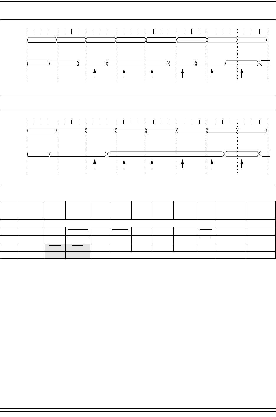
FIGURE 6-2: TIMER0 TIMING: INTERNAL CLOCK/NO PRESCALE
FIGURE 6-3: TIMER0 TIMING: INTERNAL CLOCK/PRESCALE 1:2
TABLE 6-1: REGISTERS ASSOCIATED WITH TIMER0
Addr Name Bit 7 Bit 6 Bit 5 Bit 4 Bit 3 Bit 2 Bit 1 Bit 0
Value on
Power-On
Reset
Value on
All Other
Resets
01h TMR0 Timer0 – 8-bit Real-Time Clock/Counter xxxx xxxx uuuu uuuu
08h CM1CON0 C1OUT C1OUTEN
C1POL C1T0CS C1ON C1NREF C1PREF C1WU 1111 1111
uuuu uuuu
0Bh CM2CON0 C2OUT C2OUTEN
C2POL C2PREF2 C2ON C2NREF C2PREF1 C2WU 1111 1111
uuuu uuuu
N/A OPTION
RBWU RBPU T0CS T0SE PSA PS2 PS1 PS0 1111 1111 1111 1111
N/A TRIS
(1)
— — I/O Control Register (PORTB, PORTC) --11 1111 --11 1111
Legend: Shaded cells are not used by Timer0. – = unimplemented, x = unknown, u = unchanged.
Note 1: The TRIS of the T0CKI pin is overridden when T0CS = 1.
PC – 1
Q1 Q2 Q3 Q4
Q1 Q2 Q3 Q4 Q1 Q2 Q3 Q4 Q1 Q2 Q3 Q4 Q1 Q2 Q3 Q4 Q1 Q2 Q3 Q4 Q1 Q2 Q3 Q4 Q1 Q2 Q3 Q4
Instruction
Fetch
Timer0
PC PC + 1 PC + 2 PC + 3 PC + 4 PC + 6
T0
T0 + 1 T0 + 2 NT0
NT0 + 1
NT0 + 2
MOVWF TMR0 MOVF TMR0,W MOVF TMR0,W MOVF TMR0,W MOVF TMR0,W MOVF TMR0,W
Write TMR0
executed
Read TMR0
reads NT0
Read TMR0
reads NT0
Read TMR0
reads NT0
Read TMR0
reads NT0 + 1
Read TMR0
reads NT0 + 2
Instruction
Executed
PC + 5
PC
(Program
Counter)
PC – 1
Q1 Q2 Q3 Q4
Q1 Q2 Q3 Q4 Q1 Q2 Q3 Q4 Q1 Q2 Q3 Q4 Q1 Q2 Q3 Q4 Q1 Q2 Q3 Q4 Q1 Q2 Q3 Q4 Q1 Q2 Q3 Q4
Instruction
Fetch
Timer0
PC PC + 1 PC + 2 PC + 3 PC + 4 PC + 6
T0
T0 + 1 NT0
NT0 + 1
MOVWF TMR0 MOVF TMR0,W MOVF TMR0,W MOVF TMR0,W MOVF TMR0,W MOVF TMR0,W
Write TMR0
executed
Read TMR0
reads NT0
Read TMR0
reads NT0
Read TMR0
reads NT0
Read TMR0
reads NT0 + 1
Read TMR0
reads NT0 + 2
Instruction
Executed
PC + 5
PC
(Program
Counter)

© 2009 Microchip Technology Inc. Preliminary DS41338C-page 31
MCV14A
6.1 Using Timer0 with an External
Clock
When an external clock input is used for Timer0, it must
meet certain requirements. The external clock
requirement is due to internal phase clock (TOSC)
synchronization. Also, there is a delay in the actual
incrementing of Timer0 after synchronization.
6.1.1 EXTERNAL CLOCK
SYNCHRONIZATION
When no prescaler is used, the external clock input is
the same as the prescaler output. The synchronization
of T0CKI with the internal phase clocks is accom-
plished by sampling the prescaler output on the Q2 and
Q4 cycles of the internal phase clocks (Figure 6-4).
Therefore, it is necessary for T0CKI to be high for at
least 2 T
OSC (and a small RC delay of 2 Tt0H) and low
for at least 2 T
OSC (and a small RC delay of 2 Tt0H).
Refer to the electrical specification of the desired
device.
When a prescaler is used, the external clock input is
divided by the asynchronous ripple counter-type
prescaler, so that the prescaler output is symmetrical.
For the external clock to meet the sampling require-
ment, the ripple counter must be taken into account.
Therefore, it is necessary for T0CKI to have a period of
at least 4 T
OSC (and a small RC delay of 4 Tt0H)
divided by the prescaler value. The only requirement
on T0CKI high and low time is that they do not violate
the minimum pulse width requirement of Tt0H. Refer to
parameters 40, 41 and 42 in the electrical specification
of the desired device.
6.1.2 TIMER0 INCREMENT DELAY
Since the prescaler output is synchronized with the
internal clocks, there is a small delay from the time the
external clock edge occurs to the time the Timer0
module is actually incremented. Figure 6-4 shows the
delay from the external clock edge to the timer
incrementing.
FIGURE 6-4: TIMER0 TIMING WITH EXTERNAL CLOCK
Increment Timer0 (Q4)
External Clock Input or
Q1 Q2 Q3 Q4 Q1 Q2 Q3 Q4 Q1 Q2 Q3 Q4 Q1 Q2 Q3 Q4
Timer0
T0 T0 + 1 T0 + 2
Small pulse
misses sampling
External Clock/Prescaler
Output After Sampling
(3)
Prescaler Output
(2)
(1)
Note 1: Delay from clock input change to Timer0 increment is 3 T
OSC to 7 TOSC. (Duration of Q = TOSC). Therefore, the error
in measuring the interval between two edges on Timer0 input = ±4 T
OSC max.
2: External clock if no prescaler selected; prescaler output otherwise.
3: The arrows indicate the points in time where sampling occurs.

MCV14A
DS41338C-page 32 Preliminary © 2009 Microchip Technology Inc.
6.2 Prescaler
An 8-bit counter is available as a prescaler for the
Timer0 module or as a postscaler for the Watchdog
Timer (WDT), respectively (see Section 7.6 “Watch-
dog Timer (WDT)”). For simplicity, this counter is
being referred to as “prescaler” throughout this data
sheet.
The PSA and PS<2:0> bits (OPTION<3:0>) determine
prescaler assignment and prescale ratio.
When assigned to the Timer0 module, all instructions
writing to the TMR0 register (e.g., CLRF 1, MOVWF 1,
BSF 1, x, etc.) will clear the prescaler. When assigned
to WDT, a CLRWDT instruction will clear the prescaler
along with the WDT. The prescaler is neither readable
nor writable. On a Reset, the prescaler contains all ‘0’s.
6.2.1 SWITCHING PRESCALER
ASSIGNMENT
The prescaler assignment is fully under software
control (i.e., it can be changed “on-the-fly” during
program execution). To avoid an unintended device
Reset, the following instruction sequence (Example 6-
1) must be executed when changing the prescaler
assignment from Timer0 to the WDT.
EXAMPLE 6-1: CHANGING PRESCALER
(TIMER0 → WDT)
To change the prescaler from the WDT to the Timer0
module, use the sequence shown in Example 6-2. This
sequence must be used even if the WDT is disabled. A
CLRWDT instruction should be executed before
switching the prescaler.
EXAMPLE 6-2: CHANGING PRESCALER
(WDT → TIMER0)
Note: The prescaler may be used by either the
Timer0 module or the WDT, but not both.
Thus, a prescaler assignment for the
Timer0 module means that there is no
prescaler for the WDT and vice versa.
CLRWDT ;Clear WDT
CLRF TMR0 ;Clear TMR0 & Prescaler
MOVLW ‘00xx1111’b;These 3 lines (5, 6, 7)
OPTION ;are required only if
;desired
CLRWDT ;PS<2:0> are 000 or 001
MOVLW ‘00xx1xxx’b;Set Postscaler to
OPTION ;desired WDT rate
CLRWDT ;Clear WDT and
;prescaler
MOVLW ‘xxxx0xxx’ ;Select TMR0, new
;prescale value and
;clock source
OPTION

© 2009 Microchip Technology Inc. Preliminary DS41338C-page 33
MCV14A
FIGURE 6-5: BLOCK DIAGRAM OF THE TIMER0/WDT PRESCALER
TCY (= FOSC/4)
Sync
2
Cycles
TMR0 Reg
8-bit Prescaler
8-to-1 MUX
M
MUX
Watchdog
Timer
PSA
(1)
0
1
0
1
WDT
Time-out
PS<2:0>
(1)
8
PSA
(1)
WDT Enable bit
0
1
0
1
Data Bus
8
PSA
(1)
T0CS
(1)
M
U
X
M
U
X
U
X
T0SE
(1)
Note 1: T0CS, T0SE, PSA, PS<2:0> are bits in the OPTION register.
T0CKI
Pin
0
1
C1TOCS
Comparator
Output

MCV14A
DS41338C-page 34 Preliminary © 2009 Microchip Technology Inc.
NOTES:

© 2009 Microchip Technology Inc. Preliminary DS41338C-page 35
MCV14A
7.0 SPECIAL FEATURES OF THE
CPU
What sets a microcontroller apart from other
processors are special circuits that deal with the needs
of real-time applications. The MCV14A
microcontrollers have a host of such features intended
to maximize system reliability, minimize cost through
elimination of external components, provide
power-saving operating modes and offer code
protection. These features are:
• Oscillator Selection
• Reset:
- Power-on Reset (POR)
- Device Reset Timer (DRT)
- Wake-up from Sleep on Pin Change
• Watchdog Timer (WDT)
• Sleep
• Code Protection
• ID Locations
• In-Circuit Serial Programming™
•Clock Out
The MCV14A device has a Watchdog Timer, which can
be shut off only through Configuration bit WDTE. It runs
off of its own RC oscillator for added reliability. If using
HS, XT or LP selectable oscillator options, there is
always an 18 ms (nominal) delay provided by the
Device Reset Timer (DRT), intended to keep the chip in
Reset until the crystal oscillator is stable. If using
INTRC or EXTRC, there is a 1 ms delay only on V
DD
power-up. With this timer on-chip, most applications
need no external Reset circuitry.
The Sleep mode is designed to offer a very low current
Power-Down mode. The user can wake-up from Sleep
through a change on input pins or through a Watchdog
Timer time-out. Several oscillator options are also
made available to allow the part to fit the application,
including an internal 4/8 MHz oscillator. The EXTRC
oscillator option saves system cost while the LP crystal
option saves power. A set of Configuration bits are
used to select various options.
7.1 Configuration Bits
The MCV14A Configuration Words consist of 12 bits.
Configuration bits can be programmed to select various
device configurations. Three bits are for the selection of
the oscillator type; one bit is the Watchdog Timer
enable bit, one bit is the MCLR
enable bit and one bit is
for code protection (Register 7-1).

MCV14A
DS41338C-page 36 Preliminary © 2009 Microchip Technology Inc.
REGISTER 7-1: CONFIG: CONFIGURATION WORD REGISTER
CPDF IOSCFS MCLRE CP WDTE FOSC2 FOSC1 FOSC0
bit 7 bit 0
bit 7 CP
DF: Code Protection bit – Flash Data Memory
1 = Code protection off
0 = Code protection on
bit 6 IOSCFS: Internal Oscillator Frequency Select bit
1 = 8 MHz INTOSC speed
0 = 4 MHz INTOSC speed
bit 5 MCLRE: Master Clear Enable bit
1 = RB3/MCLR
pin functions as MCLR
0 = RB3/MCLR pin functions as RB3, MCLR internally tied to VDD
bit 4 CP: Code Protection bit – User Program Memory
1 = Code protection off
0 = Code protection on
bit 3 WDTE: Watchdog Timer Enable bit
1 = WDT enabled
0 = WDT disabled
bit 2-0 FOSC<2:0>: Oscillator Selection bits
000 = LP oscillator and 18 ms DRT
001 = XT oscillator and 18 ms DRT
010 = HS oscillator and 18 ms DRT
011 = EC oscillator with RB4 function on RB4/OSC2/CLKOUT and 1 ms DRT
(1)
100 = INTRC with RB4 function on RB4/OSC2/CLKOUT and 1 ms DRT
(1)
101 = INTRC with CLKOUT function on RB4/OSC2/CLKOUT and 1 ms DRT
(1)
110 = EXTRC with RB4 function on RB4/OSC2/CLKOUT and 1 ms DRT
(1)
111 = EXTRC with CLKOUT function on RB4/OSC2/CLKOUT and 1 ms DRT
(1)
Note 1: DRT length (18 ms or 1 ms) is a function of Clock mode selection. It is the responsibility of the application
designer to ensure the use of either 18 ms (nominal) DRT or the 1 ms (nominal) DRT will result in accept-
able operation. Refer to Section 11.1 “DC Characteristics: MCV14A (Industrial)” and Section 11.2
“DC Characteristics: MCV14A” for V
DD rise time and stability requirements for this mode of operation.

© 2009 Microchip Technology Inc. Preliminary DS41338C-page 37
MCV14A
7.2 Oscillator Configurations
7.2.1 OSCILLATOR TYPES
The MCV14A device can be operated in up to six
different Oscillator modes. The user can program up to
three Configuration bits (FOSC<2:0>). To select one of
these modes:
• LP: Low-Power Crystal
• XT: Crystal/Resonator
• HS: High-Speed Crystal/Resonator
• INTRC: Internal 4/8 MHz Oscillator
• EXTRC: External Resistor/Capacitor
• EC: External High-Speed Clock Input
7.2.2 CRYSTAL OSCILLATOR/CERAMIC
RESONATORS
In HS, XT or LP modes, a crystal or ceramic resonator
is connected to the RB5/OSC1/CLKIN and
RB4/OSC2/CLKOUT pins to establish oscillation
(Figure 7-1). The MCV14A oscillator designs require
the use of a parallel cut crystal. Use of a series cut crys-
tal may give a frequency out of the crystal manufactur-
ers specifications. When in HS, XT or LP modes, the
device can have an external clock source drive the
RB5/OSC1/CLKIN pin (Figure 7-2). This pin should be
left open and unloaded. Also when using this mode, the
external clock should observe the frequency limits for
the Clock mode chosen (HS, XT or LP).
FIGURE 7-1: CRYSTAL OPERATION
(OR CERAMIC
RESONATOR)
(HS, XT OR LP OSC
CONFIGURATION)
FIGURE 7-2: EXTERNAL CLOCK INPUT
OPERATION (HS, XT, LP
OR EC OSC
CONFIGURATION)
TABLE 7-1: CAPACITOR SELECTION FOR
CERAMIC RESONATORS
Note 1: This device has been designed to
perform to the parameters of its data
sheet. It has been tested to an electrical
specification designed to determine its
conformance with these parameters.
Due to process differences in the
manufacture of this device, this device
may have different performance
characteristics than its earlier version.
These differences may cause this device
to perform differently in your application
than the earlier version of this device.
2: The user should verify that the device
oscillator starts and performs as
expected. Adjusting the loading capacitor
values and/or the Oscillator mode may
be required.
Osc
Type
Resonator
Freq.
Cap. Range
C1
Cap. Range
C2
XT 4.0 MHz 30 pF 30 pF
HS 16 MHz 10-47 pF 10-47 pF
Note 1: These values are for design guidance
only. Since each resonator has its own
characteristics, the user should consult
the resonator manufacturer for
appropriate values of external
components.
Note 1: See Capacitor Selection tables for
recommended values of C1 and C2.
2: A series resistor (RS) may be required for AT
strip cut crystals.
3: RF approx. value = 10 MΩ.
C1
(1)
C2
(1)
XTAL
OSC2
OSC1
RF
(3)
Sleep
To internal
logic
RS
(2)
MCV14A
Clock From
ext. system
MCV14A
OSC2/CLKOUT/RB4
RB5/OSC1/CLKIN
OSC2/CLKOUT/RB4
(1)
EC, HS, XT, LP
Note 1: RB4 is available in EC mode only.
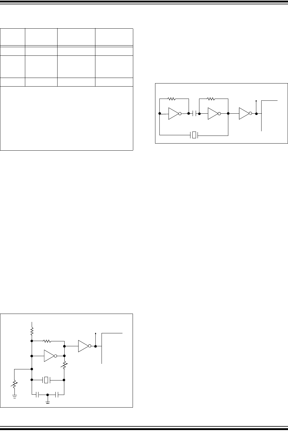
MCV14A
DS41338C-page 38 Preliminary © 2009 Microchip Technology Inc.
TABLE 7-2: CAPACITOR SELECTION FOR
CRYSTAL OSCILLATOR
(2)
7.2.3 EXTERNAL CRYSTAL OSCILLATOR
CIRCUIT
Either a prepackaged oscillator or a simple oscillator
circuit with TTL gates can be used as an external
crystal oscillator circuit. Prepackaged oscillators
provide a wide operating range and better stability. A
well-designed crystal oscillator will provide good
performance with TTL gates. Two types of crystal
oscillator circuits can be used: one with parallel
resonance, or one with series resonance.
Figure 7-3 shows implementation of a parallel resonant
oscillator circuit. The circuit is designed to use the fun-
damental frequency of the crystal. The 74AS04 inverter
performs the 180-degree phase shift that a parallel
oscillator requires. The 4.7 kΩ resistor provides the
negative feedback for stability. The 10 kΩ potentiome-
ters bias the 74AS04 in the linear region. This circuit
could be used for external oscillator designs.
FIGURE 7-3: EXTERNAL PARALLEL
RESONANT CRYSTAL
OSCILLATOR CIRCUIT
Figure 7-4 shows a series resonant oscillator circuit.
This circuit is also designed to use the fundamental
frequency of the crystal. The inverter performs a
180-degree phase shift in a series resonant oscillator
circuit. The 330 Ω resistors provide the negative
feedback to bias the inverters in their linear region.
FIGURE 7-4: EXTERNAL SERIES
RESONANT CRYSTAL
OSCILLATOR CIRCUIT
7.2.4 EXTERNAL RC OSCILLATOR
For timing insensitive applications, the RC device
option offers additional cost savings. The RC oscillator
frequency is a function of the supply voltage, the resis-
tor (R
EXT) and capacitor (CEXT) values, and the operat-
ing temperature. In addition to this, the oscillator
frequency will vary from unit-to-unit due to normal pro-
cess parameter variation. Furthermore, the difference
in lead frame capacitance between package types will
also affect the oscillation frequency, especially for low
C
EXT values. The user also needs to take into account
variation due to tolerance of external R and C
components used.
Figure 7-5 shows how the R/C combination is
connected to the MCV14A device. For R
EXT values
below 3.0 kΩ, the oscillator operation may become
unstable, or stop completely. For very high REXT values
(e.g., 1 MΩ), the oscillator becomes sensitive to noise,
humidity and leakage. Thus, we recommend keeping
R
EXT between 5.0 kΩ and 100 kΩ.
Although the oscillator will operate with no external
capacitor (C
EXT = 0 pF), we recommend using values
above 20 pF for noise and stability reasons. With no or
small external capacitance, the oscillation frequency
can vary dramatically due to changes in external
capacitances, such as PCB trace capacitance or
package lead frame capacitance.
Section 11.0 “Electrical Characteristics” shows RC
frequency variation from part-to-part due to normal
process variation. The variation is larger for larger val-
ues of R (since leakage current variation will affect RC
frequency more for large R) and for smaller values of C
(since variation of input capacitance will affect RC
frequency more).
Osc
Type
Resonator
Freq.
Cap. Range
C1
Cap. Range
C2
LP 32 kHz
(1)
15 pF 15 pF
XT 200 kHz
1 MHz
4 MHz
47-68 pF
15 pF
15 pF
47-68 pF
15 pF
15 pF
HS 20 MHz 15-47 pF 15-47 pF
Note 1: For V
DD > 4.5V, C1 = C2 ≈ 30 pF is
recommended.
2: These values are for design guidance
only. Rs may be required to avoid over-
driving crystals with low drive level specifi-
cation. Since each crystal has its own
characteristics, the user should consult
the crystal manufacturer for appropriate
values of external components.
20 pF
+5V
20 pF
10k
4.7k
10k
74AS04
XTAL
10k
74AS04
CLKIN
To Other
Devices
MCV14A
330
74AS04
74AS04
MCV14A
CLKIN
To Other
Devices
XTAL
330
74AS04
0.1 mF

© 2009 Microchip Technology Inc. Preliminary DS41338C-page 39
MCV14A
Also, see the Electrical Specifications section for
variation of oscillator frequency due to V
DD for given
R
EXT/CEXT values, as well as frequency variation due
to operating temperature for given R, C and V
DD
values.
FIGURE 7-5: EXTERNAL RC
OSCILLATOR MODE
7.2.5 INTERNAL 4/8 MHz RC
OSCILLATOR
The internal RC oscillator provides a fixed 4/8 MHz
(nominal) system clock at V
DD = 5V and 25°C, (see
Section 11.0 “Electrical Characteristics” for
information on variation over voltage and temperature).
In addition, a calibration instruction is programmed into
the last address of memory, which contains the
calibration value for the internal RC oscillator. This
location is always non-code protected, regardless of
the code-protect settings. This value is programmed as
a MOVLW XX instruction where XX is the calibration
value, and is placed at the Reset vector. This will load
the W register with the calibration value upon Reset
and the PC will then roll over to the users program at
address 0x000. The user then has the option of writing
the value to the OSCCAL Register (05h) or ignoring it.
OSCCAL, when written to with the calibration value, will
“trim” the internal oscillator to remove process variation
from the oscillator frequency.
For the MCV14A device, only bits <7:1> of OSCCAL
are used for calibration. See Register 3-3 for more
information.
VDD
REXT
CEXT
VSS
OSC1
Internal
clock
N
FOSC/4
OSC2/CLKOUT
MCV14A
Note: Erasing the device will also erase the
pre-programmed internal calibration value
for the internal oscillator. The calibration
value must be read prior to erasing the
part so it can be reprogrammed correctly
later.
Note: The bit 0 of the OSCCAL register is
unimplemented and should be written as
‘0’ when modifying OSCCAL for
compatibility with future devices.

MCV14A
DS41338C-page 40 Preliminary © 2009 Microchip Technology Inc.
7.3 Reset
The device differentiates between various kinds of
Reset:
• Power-on Reset (POR)
•MCLR
Reset during normal operation
•MCLR
Reset during Sleep
• WDT Time-out Reset during normal operation
• WDT Time-out Reset during Sleep
• Wake-up from Sleep on pin change
Some registers are not reset in any way, they are
unknown on POR and unchanged in any other Reset.
Most other registers are reset to “Reset state” on
Power-on Reset (POR), MCLR
, WDT or Wake-up on
pin change Reset during normal operation. They are
not affected by a WDT Reset during Sleep or MCLR
Reset during Sleep, since these Resets are viewed as
resumption of normal operation. The exceptions to this
are TO, PD and RBWUF bits. They are set or cleared
differently in different Reset situations. These bits are
used in software to determine the nature of Reset. See
Table 7-3 for a full description of Reset states of all
registers.
TABLE 7-3: RESET CONDITIONS FOR REGISTERS
Register Address Power-on Reset
MCLR
Reset, WDT Time-out,
Wake-up On Pin Change
W — qqqq qqq0
(1)
qqqq qqq0
(1)
INDF 00h xxxx xxxx uuuu uuuu
TMR0 01h xxxx xxxx uuuu uuuu
PCL 02h 1111 1111 1111 1111
STATUS 03h 0001 1xxx qq0q quuu
(2)
FSR 04h 100x xxxx 1uuu uuuu
OSCCAL 05h 1111 111- uuuu uuu-
PORTB 06h --xx xxxx --uu uuuu
PORTC 07h --xx xxxx --uu uuuu
CMICON0 08h q111 1111 quuu uuuu
ADCON0 09h 1111 1100 1111 1100
ADRES 0Ah xxxx xxxx uuuu uuuu
CM2CON0 0Bh q111 1111 quuu uuuu
VRCON 0Ch 001-1111 uuu-uuuu
OPTION — 1111 1111 1111 1111
TRISB — --11 1111 --11 1111
TRISC — --11 1111 --11 1111
EECON 21h/61h ---0 x000 ---0 q000
EEDATA 25h/65h xxxx xxxx uuuu uuuu
EEADR 26h/66h --xx xxxx --uu uuuu
Legend: u = unchanged, x = unknown, – = unimplemented bit, read as ‘0’, q = value depends on condition.
Note 1: Bits <7:1> of W register contain oscillator calibration values due to MOVLW XX instruction at top of
memory.
2: See Table 7-4 for Reset value for specific conditions.

© 2009 Microchip Technology Inc. Preliminary DS41338C-page 41
MCV14A
TABLE 7-4: RESET CONDITION FOR SPECIAL REGISTERS
STATUS Addr: 03h PCL Addr: 02h
Power-on Reset 0001 1xxx 1111 1111
MCLR Reset during normal operation 000u uuuu 1111 1111
MCLR
Reset during Sleep 0001 0uuu 1111 1111
WDT Reset during Sleep 0000 0uuu 1111 1111
WDT Reset normal operation 0000 uuuu 1111 1111
Wake-up from Sleep on pin change 1001 0uuu 1111 1111
Legend: u = unchanged, x = unknown, – = unimplemented bit, read as ‘0’.
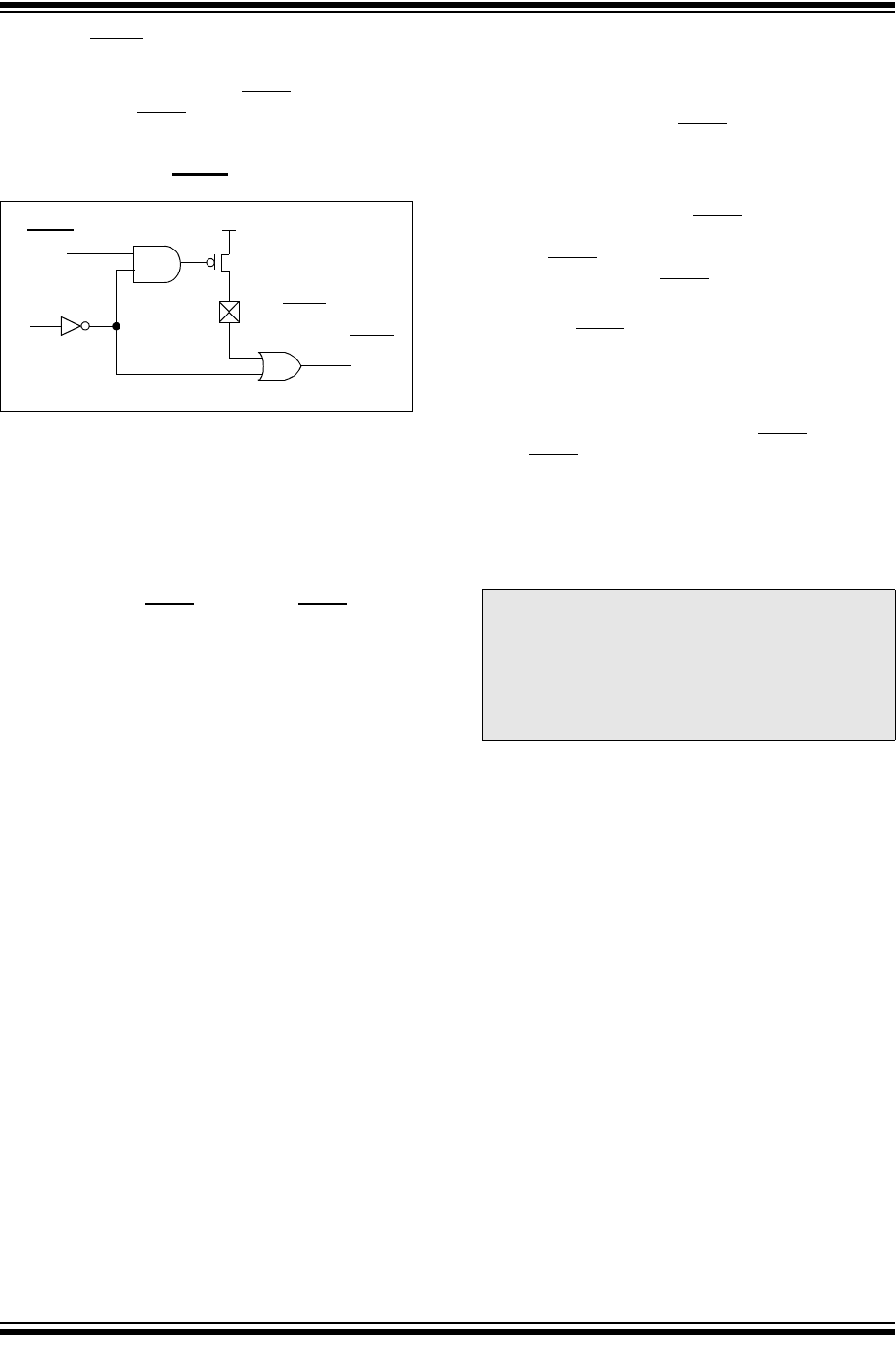
MCV14A
DS41338C-page 42 Preliminary © 2009 Microchip Technology Inc.
7.3.1 MCLR ENABLE
This Configuration bit, when unprogrammed (left in the
‘1’ state), enables the external MCLR
function. When
programmed, the MCLR
function is tied to the internal
V
DD and the pin is assigned to be a I/O. See Figure 7-6.
FIGURE 7-6: MCLR SELECT
7.4 Power-on Reset (POR)
The MCV14A device incorporates an on-chip
Power-on Reset (POR) circuitry, which provides an
internal chip Reset for most power-up situations.
The on-chip POR circuit holds the chip in Reset until
V
DD has reached a high enough level for proper
operation. To take advantage of the internal POR,
program the RB3/MCLR/VPP pin as MCLR and tie
through a resistor to V
DD, or program the pin as RB3.
An internal weak pull-up resistor is implemented using
a transistor (refer to Table 11-5 for the pull-up resistor
ranges). This will eliminate external RC components
usually needed to create a Power-on Reset. A
maximum rise time for V
DD is specified. See
Section 11.0 “Electrical Characteristics” for details.
When the device starts normal operation (exit the
Reset condition), device operating parameters
(voltage, frequency, temperature,...) must be met to
ensure operation. If these conditions are not met, the
device must be held in Reset until the operating
parameters are met.
A simplified block diagram of the on-chip Power-on
Reset circuit is shown in Figure 7-7.
The Power-on Reset circuit and the Device Reset
Timer (see Section 7.5 “Device Reset Timer (DRT)”)
circuit are closely related. On power-up, the Reset latch
is set and the DRT is reset. The DRT timer begins
counting once it detects MCLR
to be high. After the
time-out period, which is typically 18 ms or 1 ms, it will
reset the Reset latch and thus end the on-chip Reset
signal.
A power-up example where MCLR
is held low is shown
in Figure 7-8. V
DD is allowed to rise and stabilize before
bringing MCLR
high. The chip will actually come out of
Reset T
DRT msec after MCLR goes high.
In Figure 7-9, the on-chip Power-on Reset feature is
being used (MCLR and VDD are tied together or the pin
is programmed to be RB3. The V
DD is stable before the
start-up timer times out and there is no problem in get-
ting a proper Reset. However, Figure 7-10 depicts a
problem situation where V
DD rises too slowly. The time
between when the DRT senses that MCLR
is high and
when MCLR
and VDD actually reach their full value, is
too long. In this situation, when the start-up timer times
out, V
DD has not reached the VDD (min) value and the
chip may not function correctly. For such situations, we
recommend that external RC circuits be used to
achieve longer POR delay times (Figure 7-9).
For additional information, refer to Application Notes
AN522, “Power-Up Considerations” (DS00522) and
AN607, “Power-up Trouble Shooting” (DS00607).
RB3/MCLR/VPP
MCLRE
Internal MCLR
RBWU
Note: When the device starts normal operation
(exit the Reset condition), device
operating parameters (voltage, frequency,
temperature, etc.) must be met to ensure
operation. If these conditions are not met,
the device must be held in Reset until the
operating conditions are met.

© 2009 Microchip Technology Inc. Preliminary DS41338C-page 43
MCV14A
FIGURE 7-7: SIMPLIFIED BLOCK DIAGRAM OF ON-CHIP RESET CIRCUIT
FIGURE 7-8: TIME-OUT SEQUENCE ON POWER-UP (MCLR
PULLED LOW)
FIGURE 7-9: TIME-OUT SEQUENCE ON POWER-UP (MCLR
TIED TO VDD): FAST VDD RISE
TIME
SQ
R
Q
VDD
RB3/MCLR/VPP
Power-up
Detect
POR (Power-on Reset)
WDT Reset
CHIP Reset
MCLRE
Wake-up on pin Change Reset
Start-up Timer
(10 μs, 1.125 ms
WDT Time-out
Pin Change
Sleep
MCLR
Reset
or 18 ms)
VDD
MCLR
Internal POR
DRT Time-out
Internal Reset
TDRT
VDD
MCLR
Internal POR
DRT Time-out
Internal Reset
TDRT

MCV14A
DS41338C-page 44 Preliminary © 2009 Microchip Technology Inc.
FIGURE 7-10: TIME-OUT SEQUENCE ON POWER-UP (MCLR TIED TO VDD): SLOW VDD RISE
TIME
VDD
MCLR
Internal POR
DRT Time-out
Internal Reset
TDRT
V1
Note: When VDD rises slowly, the TDRT time-out expires long before VDD has reached its final
value. In this example, the chip will reset properly if, and only if, V1 ≥ V
DD min.

© 2009 Microchip Technology Inc. Preliminary DS41338C-page 45
MCV14A
7.5 Device Reset Timer (DRT)
On the MCV14A device, the DRT runs any time the
device is powered up. DRT runs from Reset and varies
based on oscillator selection and Reset type (see
Table 7-5).
The DRT operates on an internal RC oscillator. The
processor is kept in Reset as long as the DRT is active.
The DRT delay allows V
DD to rise above VDD min. and
for the oscillator to stabilize.
Oscillator circuits based on crystals or ceramic
resonators require a certain time after power-up to
establish a stable oscillation. The on-chip DRT keeps
the device in a Reset condition after MCLR
has reached
a logic high (V
IH MCLR) level. Programming
RB3/MCLR
/VPP as MCLR and using an external RC
network connected to the MCLR
input is not required in
most cases. This allows savings in cost-sensitive and/or
space restricted applications, as well as allowing the use
of the RB3/MCLR
/VPP pin as a general purpose input.
The Device Reset Time delays will vary from
chip-to-chip due to V
DD, temperature and process
variation. See AC parameters for details.
The DRT will also be triggered upon a Watchdog Timer
time-out from Sleep. This is particularly important for
applications using the WDT to wake from Sleep mode
automatically.
Reset sources are POR, MCLR
, WDT time-out and
wake-up on pin change. See Section 7.8.2 “Wake-up
from Sleep”, Notes 1, 2 and 3.
7.6 Watchdog Timer (WDT)
The Watchdog Timer (WDT) is a free running on-chip
RC oscillator, which does not require any external
components. This RC oscillator is separate from the
external RC oscillator of the RB5/OSC1/CLKIN pin and
the internal 4/8 MHz oscillator. This means that the
WDT will run even if the main processor clock has been
stopped, for example, by execution of a SLEEP instruc-
tion. During normal operation or Sleep, a WDT Reset or
wake-up Reset, generates a device Reset.
The TO
bit (STATUS<4>) will be cleared upon a
Watchdog Timer Reset.
The WDT can be permanently disabled by
programming the configuration WDTE as a ‘0’ (see
Section 7.1 “Configuration Bits”). Refer to the
MCV14A Programming Specifications to determine
how to access the Configuration Word.
TABLE 7-5: TYPICAL DRT PERIODS
7.6.1 WDT PERIOD
The WDT has a nominal time-out period of 18 ms, (with
no prescaler). If a longer time-out period is desired, a
prescaler with a division ratio of up to 1:128 can be
assigned to the WDT (under software control) by
writing to the OPTION register. Thus, a time-out period
of a nominal 2.3 seconds can be realized. These
periods vary with temperature, V
DD and part-to-part
process variations (see DC specs).
Under worst-case conditions (V
DD = Min., Temperature
= Max., max. WDT prescaler), it may take several
seconds before a WDT time-out occurs.
7.6.2 WDT PROGRAMMING
CONSIDERATIONS
The CLRWDT instruction clears the WDT and the
postscaler, if assigned to the WDT, and prevents it from
timing out and generating a device Reset.
The SLEEP instruction resets the WDT and the
postscaler, if assigned to the WDT. This gives the
maximum Sleep time before a WDT wake-up Reset.
Oscillator
Configuration
POR Reset
Subsequent
Resets
HS, XT, LP 18 ms 18 ms
EC 1.125 ms 10 μs
INTOSC, EXTRC 1.125 ms 10 μs
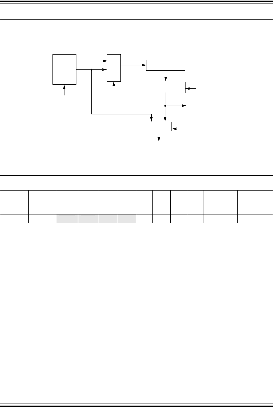
MCV14A
DS41338C-page 46 Preliminary © 2009 Microchip Technology Inc.
FIGURE 7-11: WATCHDOG TIMER BLOCK DIAGRAM
TABLE 7-6: SUMMARY OF REGISTERS ASSOCIATED WITH THE WATCHDOG TIMER
Address Name Bit 7 Bit 6 Bit 5 Bit 4 Bit 3 Bit 2 Bit 1 Bit 0
Value on
Power-On
Reset
Value on
All Other
Resets
N/A OPTION
RBWU RBPU T0CS T0SE PSA PS2 PS1 PS0 1111 1111 1111 1111
Legend: Shaded boxes = Not used by Watchdog Timer.
(Figure 6-1)
Postscaler
Note 1: PSA, PS<2:0> are bits in the OPTION register.
WDT Time-out
Watchdog
Time
From Timer0 Clock Source
WDT Enable
Configuration
Bit
PSA
Postscaler
8-to-1 MUX
PS<2:0>
(1)
(Figure 6-4)
To Timer0
0
1
M
U
X
1
0
PSA
(1)
MUX

© 2009 Microchip Technology Inc. Preliminary DS41338C-page 47
MCV14A
7.7 Time-out Sequence, Power-down
and Wake-up from Sleep Status
Bits (TO
, PD, RBWUF)
The TO, PD and RBWUF bits in the STATUS register
can be tested to determine if a Reset condition has
been caused by a power-up condition, a MCLR or
Watchdog Timer (WDT) Reset.
TABLE 7-7: TO/PD/RBWUF STATUS
AFTER RESET
7.8 Power-down Mode (Sleep)
A device may be powered down (Sleep) and later
powered up (wake-up from Sleep).
7.8.1 SLEEP
The Power-Down mode is entered by executing a
SLEEP instruction.
If enabled, the Watchdog Timer will be cleared but
keeps running, the TO
bit (STATUS<4>) is set, the PD
bit (STATUS<3>) is cleared and the oscillator driver is
turned off. The I/O ports maintain the status they had
before the SLEEP instruction was executed (driving
high, driving low or high-impedance).
For lowest current consumption while powered down,
the T0CKI input should be at V
DD or VSS and the
RB3/MCLR
/VPP pin must be at a logic high level if
MCLR
is enabled.
7.8.2 WAKE-UP FROM SLEEP
The device can wake-up from Sleep through one of
the following events:
1. An external Reset input on RB3/MCLR
/VPP pin,
when configured as MCLR
.
2. A Watchdog Timer Time-out Reset (if WDT was
enabled).
3. A change on input pin RB0, RB1, RB3 or RB4
when wake-up on change is enabled.
These events cause a device Reset. The TO
, PD and
RBWUF bits can be used to determine the cause of
device Reset. The TO bit is cleared if a WDT time-out
occurred (and caused wake-up). The PD
bit, which is
set on power-up, is cleared when SLEEP is invoked.
The RBWUF bit indicates a change in state while in
Sleep at pins RB0, RB1, RB3 or RB4 (since the last file
or bit operation on RB port).
The WDT is cleared when the device wakes from
Sleep, regardless of the wake-up source.
RBWUF TO PD Reset Caused By
000WDT wake-up from Sleep
00uWDT time-out (not from
Sleep)
010MCLR
wake-up from Sleep
011Power-up
0uuMCLR
not during Sleep
110Wake-up from Sleep on pin
change
Legend: u = unchanged
Note 1: The TO
, PD and RBWUF bits maintain
their status (u) until a Reset occurs. A
low-pulse on the MCLR input does not
change the TO
, PD and RBWUF Status
bits.
Note: A Reset generated by a WDT time-out
does not drive the MCLR
pin low.
Note: Caution: Right before entering Sleep,
read the input pins. When in Sleep,
wake-up occurs when the values at the
pins change from the state they were in at
the last reading. If a wake-up on change
occurs and the pins are not read before
re-entering Sleep, a wake-up will occur
immediately even if no pins change while
in Sleep mode.

MCV14A
DS41338C-page 48 Preliminary © 2009 Microchip Technology Inc.
7.9 Program Verification/Code
Protection
If the code protection bit has not been programmed, the
on-chip program memory can be read out for
verification purposes.
The first 64 locations and the last location (OSCCAL)
can be read, regardless of the code protection bit
setting.
The last memory location can be read regardless of the
code protection bit setting on the MCV14A device.
7.10 ID Locations
Four memory locations are designated as ID locations
where the user can store checksum or other code
identification numbers. These locations are not
accessible during normal execution, but are readable
and writable during Program/Verify.
Use only the lower 4 bits of the ID locations and always
program the upper 8 bits as ‘0’s.
7.11 In-Circuit Serial Programming™
The MCV14A microcontroller can be serially
programmed while in the end application circuit. This is
simply done with two lines for clock and data, and three
other lines for power, ground and the programming
voltage. This allows customers to manufacture boards
with unprogrammed devices and then program the
microcontroller just before shipping the product. This
also allows the most recent firmware, or a custom
firmware, to be programmed.
The devices are placed into a Program/Verify mode by
holding the RB1 and RB0 pins low while raising the
MCLR
(VPP) pin from VIL to VIHH. RB1 becomes the
programming clock and B0 becomes the programming
data. Both RB1 and RB0 are Schmitt Trigger inputs in
this mode.
After Reset, a 6-bit command is then supplied to the
device. Depending on the command, 14 bits of program
data are then supplied to or from the device, depending
if the command was a Load or a Read.
A typical In-Circuit Serial Programming connection is
shown in Figure 7-12.
FIGURE 7-12: TYPICAL IN-CIRCUIT
SERIAL PROGRAMMING
CONNECTION
External
Connector
Signals
To Normal
Connections
To Normal
Connections
V
DD
VSS
MCLR/VPP
RB1
RB0
+5V
0V
V
PP
CLK
Data I/O
V
DD
MCV14A

© 2009 Microchip Technology Inc. Preliminary DS41338C-page 49
MCV14A
8.0 ANALOG-TO-DIGITAL (A/D)
CONVERTER
The A/D Converter allows conversion of an analog
signal into an 8-bit digital signal.
8.1 Clock Divisors
The ADC has 4 clock source settings ADCS<1:0>.
There are 3 divisor values 16, 8 and 4. The fourth
setting is INTOSC with a divisor of 4. These settings
will allow a proper conversion when using an external
oscillator at speeds from 20 MHz to 350 kHz. Using an
external oscillator at a frequency below 350 kHz
requires the ADC oscillator setting to be INTOSC/4
(ADCS<1:0> = 11) for valid ADC results.
The ADC requires 13 T
AD periods to complete a
conversion. The divisor values do not affect the number
of TAD periods required to perform a conversion. The
divisor values determine the length of the T
AD period.
When the ADCS<1:0> bits are changed while an ADC
conversion is in process, the new ADC clock source will
not be selected until the next conversion is started. This
clock source selection will be lost when the device
enters Sleep.
8.1.1 VOLTAGE REFERENCE
There is no external voltage reference for the ADC. The
ADC reference voltage will always be V
DD.
8.1.2 ANALOG MODE SELECTION
The ANS<1:0> bits are used to configure pins for
analog input. Upon any Reset, ANS<1:0> defaults to
11. This configures pins AN0, AN1 and AN2 as analog
inputs. The comparator output, C1OUT, will override
AN2 as an input if the comparator output is enabled.
Pins configured as analog inputs are not available for
digital output. Users should not change the ANS bits
while a conversion is in process. ANS bits are active
regardless of the condition of ADON.
8.1.3 ADC CHANNEL SELECTION
The CHS bits are used to select the analog channel to
be sampled by the ADC. The CHS<1:0> bits can be
changed at any time without adversely effecting a con-
version. To acquire an analog signal the CHS<1:0>
selection must match one of the pin(s) selected by the
ANS<1:0> bits. When the ADC is on (ADON = 1) and a
channel is selected that is also being used by the
comparator, then both the comparator and the ADC will
see the analog voltage on the pin.
When the CHS<1:0> bits are changed during an ADC
conversion, the new channel will not be selected until
the current conversion is completed. This allows the
current conversion to complete with valid results. All
channel selection information will be lost when the
device enters Sleep.
TABLE 8-1: CHANNEL SELECT (ADCS)
BITS AFTER AN EVENT
8.1.4 THE GO/DONE
BIT
The GO/DONE bit is used to determine the status of a
conversion, to start a conversion and to manually halt
a conversion in process. Setting the GO/DONE
bit
starts a conversion. When the conversion is complete,
the ADC module clears the GO/DONE bit. A
conversion can be terminated by manually clearing the
GO/DONE bit while a conversion is in process. Manual
termination of a conversion may result in a partially
converted result in ADRES.
The GO/DONE
bit is cleared when the device enters
Sleep, stopping the current conversion. The ADC does
not have a dedicated oscillator, it runs off of the
instruction clock. Therefore, no conversion can occur in
sleep.
The GO/DONE
bit cannot be set when ADON is clear.
Note: The ADC clock is derived from the
instruction clock. The ADCS divisors are
then applied to create the ADC clock
Note: It is the users responsibility to ensure that
use of the ADC and comparator
simultaneously on the same pin, does not
adversely affect the signal being
monitored or adversely effect device
operation.
Event ADCS<1:0>
MCLR 11
Conversion completed CS<1:0>
Conversion terminated CS<1:0>
Power-on 11
Wake from Sleep 11

MCV14A
DS41338C-page 50 Preliminary © 2009 Microchip Technology Inc.
8.1.5 SLEEP
This ADC does not have a dedicated ADC clock, and
therefore, no conversion in Sleep is possible. If a
conversion is underway and a Sleep command is
executed, the GO/DONE
and ADON bit will be cleared.
This will stop any conversion in process and power-
down the ADC module to conserve power. Due to the
nature of the conversion process, the ADRES may con-
tain a partial conversion. At least 1 bit must have been
converted prior to Sleep to have partial conversion data
in ADRES. The ADCS and CHS bits are reset to their
default condition; ANS<1:0> = 11 and CHS<1:0> = 11.
• For accurate conversions, T
AD must meet the
following:
•500ns < T
AD < 50 μs
•TAD = 1/(FOSC/divisor)
Shaded areas indicate T
AD out of range for accurate
conversions. If analog input is desired at these
frequencies, use INTOSC/8 for the ADC clock source.
TABLE 8-2: TAD FOR ADCS SETTINGS WITH VARIOUS OSCILLATORS
TABLE 8-3: EFFECTS OF SLEEP ON ADCON0
Source
ADCS
<1:0>
Divisor
20
MHz
16
MHz
8MHz 4MHz 1MHz
500
kHz
350
kHz
200
kHz
100
kHz
32 kHz
INTOSC 11 4
— —.5μs1μs — — — — — —
FOSC 10 4 .2 μs .25 μs.5μs1μs4μs8μs11μs20μs40μs 125 μs
FOSC 01 8
.4 μs.5μs1μs2μs8μs16μs23μs40μs 80 μs 250 μs
FOSC 00 16 .8 μs1μs2μs4μs16μs32μs46μs 80 μs 160 μs 500 μs
ANS1 ANS0 ADCS1 ADCS0 CHS1 CHS0 GO/DONE ADON
Entering
Sleep
Unchanged Unchanged 111100
Wake or
Reset
11111100

© 2009 Microchip Technology Inc. Preliminary DS41338C-page 51
MCV14A
8.1.6 ANALOG CONVERSION RESULT
REGISTER
The ADRES register contains the results of the last
conversion. These results are present during the
sampling period of the next analog conversion process.
After the sampling period is over, ADRES is cleared
(= 0). A ‘leading one’ is then right shifted into the
ADRES to serve as an internal conversion complete
bit. As each bit weight, starting with the MSB, is
converted, the leading one is shifted right and the
converted bit is stuffed into ADRES. After a total of 9
right shifts of the ‘leading one’ have taken place, the
conversion is complete; the ‘leading one’ has been
shifted out and the GO/DONE
bit is cleared.
If the GO/DONE
bit is cleared in software during a
conversion, the conversion stops. The data in ADRES
is the partial conversion result. This data is valid for the
bit weights that have been converted. The position of
the ‘leading one’ determines the number of bits that
have been converted. The bits that were not converted
before the GO/DONE
was cleared are unrecoverable.
REGISTER 8-1: ADCON0: A/D CONTROL REGISTER
R/W-1 R/W-1 R/W-1 R/W-1 R/W-1 R/W-1 R/W-0 R/W-0
ANS1 ANS0 ADCS1 ADCS0 CHS1 CHS0 GO/DONE
ADON
bit 7 bit 0
Legend:
R = Readable bit W = Writable bit U = Unimplemented bit, read as ‘0’
-n = Value at POR ‘1’ = Bit is set ‘0’ = Bit is cleared x = Bit is unknown
bit 7-6 ANS<1:0>: ADC Analog Input Pin Select bits
(1), (2), (5)
00 = No pins configured for analog input
01 = AN2 configured as an analog input
10 = AN2 and AN0 configured as analog inputs
11 = AN2, AN1 and AN0 configured as analog inputs
bit 5-4 ADCS<1:0>: ADC Conversion Clock Select bits
00 = F
OSC/16
01 = F
OSC/8
10 = F
OSC/4
11 = INTOSC/4
bit 3-2 CHS<1:0>: ADC Channel Select bits
(3, 5)
00 = Channel AN0
01 = Channel AN1
10 = Channel AN2
11 = 0.6V absolute voltage reference
bit 1 GO/DONE
: ADC Conversion Status bit
(4)
1 = ADC conversion in progress. Setting this bit starts an ADC conversion cycle. This bit is automatically cleared
by hardware when the ADC is done converting.
0 = ADC conversion completed/not in progress. Manually clearing this bit while a conversion is in process termi-
nates the current conversion.
bit 0 ADON: ADC Enable bit
1 = ADC module is operating
0 = ADC module is shut-off and consumes no power
Note 1: When the ANS bits are set, the channels selected will automatically be forced into Analog mode, regardless of the pin
function previously defined. The only exception to this is the comparator, where the analog input to the comparator and
the ADC will be active at the same time. It is the users responsibility to ensure that the ADC loading on the comparator
input does not affect their application.
2: The ANS<1:0> bits are active regardless of the condition of ADON.
3: CHS<1:0> bits default to 11 after any Reset.
4: If the ADON bit is clear, the GO/DONE
bit cannot be set.
5: C1OUT, when enabled, overrides AN2.

MCV14A
DS41338C-page 52 Preliminary © 2009 Microchip Technology Inc.
EXAMPLE 8-1: PERFORMING AN
ANALOG-TO-DIGITAL
CONVERSION
EXAMPLE 8-2: CHANNEL SELECTION
CHANGE DURING
CONVERSION
REGISTER 8-2: ADRES: ADDRESS REGISTER
R/W-X R/W-X R/W-X R/W-X R/W-X R/W-X R/W-X R/W-X
ADRES7 ADRES6 ADRES5 ADRES4 ADRES3 ADRES2 ADRES1 ADRES0
bit 7 bit 0
Legend:
R = Readable bit W = Writable bit U = Unimplemented bit, read as ‘0’
-n = Value at POR ‘1’ = Bit is set ‘0’ = Bit is cleared x = Bit is unknown
;Sample code operates out of BANK0
MOVLW 0xF1 ;configure A/D
MOVWF ADCON0
BSF ADCON0, 1 ;start conversion
loop0 BTFSC ADCON0, 1;wait for ‘DONE’
GOTO loop0
MOVF ADRES, W ;read result
MOVWF result0 ;save result
BSF ADCON0, 2 ;setup for read of
;channel 1
BSF ADCON0, 1 ;start conversion
loop1 BTFSC ADCON0, 1;wait for ‘DONE’
GOTO loop1
MOVF ADRES, W ;read result
MOVWF result1 ;save result
BSF ADCON0, 3 ;setup for read of
BCF ADCON0, 2 ;channel 2
BSF ADCON0, 1 ;start conversion
loop2 BTFSC ADCON0, 1;wait for ‘DONE’
GOTO loop2
MOVF ADRES, W ;read result
MOVWF result2 ;save result
MOVLW 0xF1 ;configure A/D
MOVWF ADCON0
BSF ADCON0, 1 ;start conversion
BSF ADCON0, 2 ;setup for read of
;channel 1
loop0 BTFSC ADCON0, 1;wait for ‘DONE’
GOTO loop0
MOVF ADRES, W ;read result
MOVWF result0 ;save result
BSF ADCON0, 1 ;start conversion
BSF ADCON0, 3 ;setup for read of
BCF ADCON0, 2 ;channel 2
loop1 BTFSC ADCON0, 1;wait for ‘DONE’
GOTO loop1
MOVF ADRES, W ;read result
MOVWF result1 ;save result
BSF ADCON0, 1 ;start conversion
loop2 BTFSC ADCON0, 1;wait for ‘DONE’
GOTO loop2
MOVF ADRES, W ;read result
MOVWF result2 ;save result
CLRF ADCON0 ;optional: returns
;pins to Digital mode and turns off
;the ADC module

© 2009 Microchip Technology Inc. Preliminary DS41338C-page 53
MCV14A
9.0 COMPARATOR(S)
This device contains two comparators and a
comparator voltage reference.
REGISTER 9-1: CM1CON0: COMPARATOR C1 CONTROL REGISTER
R-1 R/W-1 R/W-1 R/W-1 R/W-1 R/W-1 R/W-1 R/W-1
C1OUT C1OUTEN
C1POL C1T0CS C1ON C1NREF C1PREF C1WU
bit 7 bit 0
Legend:
R = Readable bit W = Writable bit U = Unimplemented bit, read as ‘0’
-n = Value at POR ‘1’ = Bit is set ‘0’ = Bit is cleared x = Bit is unknown
bit 7 C1OUT: Comparator Output bit
1 = V
IN+ > VIN-
0 = V
IN+ < VIN-
bit 6 C1OUTEN
: Comparator Output Enable bit
(1), (2)
1 = Output of comparator is NOT placed on the C1OUT pin
0 = Output of comparator is placed in the C1OUT pin
bit 5 C1POL: Comparator Output Polarity bit
(2)
1 = Output of comparator is not inverted
0 = Output of comparator is inverted
bit 4 C1T0CS
: Comparator TMR0 Clock Source bit
(2)
1 = TMR0 clock source selected by T0CS control bit
0 = Comparator output used as TMR0 clock source
bit 3 C1ON: Comparator Enable bit
1 = Comparator is on
0 = Comparator is off
bit 2 C1NREF: Comparator Negative Reference Select bit
(2)
1 = C1IN- pin
0 = 0.6V V
REF
bit 1 C1PREF: Comparator Positive Reference Select bit
(2)
1 = C1IN+ pin
0 = C1IN- pin
bit 0 C1WU
: Comparator Wake-up On Change Enable bit
(2)
1 = Wake-up On Comparator Change is disabled
0 = Wake-up On Comparator Change is enabled
Note 1: Overrides T0CS bit for TRIS control of RB2.
2: When comparator is turned on, these control bits assert themselves. Otherwise, the other registers have
precedence.

MCV14A
DS41338C-page 54 Preliminary © 2009 Microchip Technology Inc.
REGISTER 9-2: CM2CON0: COMPARATOR C2 CONTROL REGISTER
R-1 R/W-1 R/W-1 R/W-1 R/W-1 R/W-1 R/W-1 R/W-1
C2OUT C2OUTEN
C2POL C2PREF2 C2ON C2NREF C2PREF1 C2WU
bit 7 bit 0
Legend:
R = Readable bit W = Writable bit U = Unimplemented bit, read as ‘0’
-n = Value at POR ‘1’ = Bit is set ‘0’ = Bit is cleared x = Bit is unknown
bit 7 C2OUT: Comparator Output bit
1 = V
IN+ > VIN-
0 = V
IN+ < VIN-
bit 6 C2OUTEN
: Comparator Output Enable bit
(1), (2)
1 = Output of comparator is NOT placed on the C2OUT pin
0 = Output of comparator is placed in the C2OUT pin
bit 5 C2POL: Comparator Output Polarity bit
(2)
1 = Output of comparator not inverted
0 = Output of comparator inverted
bit 4 C2PREF2: Comparator Positive Reference Select bit
(2)
1 = C1IN+ pin
0 = C2IN- pin
bit 3 C2ON: Comparator Enable bit
1 = Comparator is on
0 = Comparator is off
bit 2 C2NREF: Comparator Negative Reference Select bit
(2)
1 = C2IN- pin
0 = CV
REF
bit 1 C2PREF1: Comparator Positive Reference Select bit
(2)
1 = C2IN+ pin
0 = C2PREF2 controls analog input selection
bit 0 C2WU
: Comparator Wake-up on Change Enable bit
(2)
1 = Wake-up on Comparator change is disabled
0 = Wake-up on Comparator change is enabled.
Note 1: Overrides TOCS bit for TRIS control of RC4.
2: When comparator is turned on, these control bits assert themselves. Otherwise, the other registers have
precedence.

© 2009 Microchip Technology Inc. Preliminary DS41338C-page 55
MCV14A
FIGURE 9-1: COMPARATORS BLOCK DIAGRAM
+
-
C1IN+
C1IN-
VREF
(0.6V)
C1ON
C1POL
C1T0CS
RB2/C1OUT
C1OUTEN
C1OUT (Register)
T0CKI Pin
T0CKI
QD
S
READ
CM1CON0
C1WU
C1PREF
C1NREF
+
-
C2IN+
C2IN-
C2ON
C2POL
C2PREF1
C2NREF
CV
REF
C2PREF2
RC4/C2OUT
C2OUTEN
C2OUT (Register)
QD
S
CWUF
READ
CM2CON0
C2WU
1
0
1
0
1
0
1
0
1
0
1
0

MCV14A
DS41338C-page 56 Preliminary © 2009 Microchip Technology Inc.
9.1 Comparator Operation
A single comparator is shown in Figure 9-2 along with
the relationship between the analog input levels and
the digital output. When the analog input at V
IN+ is less
than the analog input V
IN-, the output of the comparator
is a digital low level. The shaded area of the output of
the comparator in Figure 9-2 represent the uncertainty
due to input offsets and response time. See Table 11-2
for Common Mode Voltage.
FIGURE 9-2: SINGLE COMPARATOR
9.2 Comparator Reference
An internal reference signal may be used depending on
the comparator operating mode. The analog signal that
is present at V
IN- is compared to the signal at VIN+, and
the digital output of the comparator is adjusted accord-
ingly (Figure 9-2). Please see Section 10.0 “Compar-
ator Voltage Reference Module” for internal
reference specifications.
9.3 Comparator Response Time
Response time is the minimum time after selecting a
new reference voltage or input source before the
comparator output is to have a valid level. If the
comparator inputs are changed, a delay must be used
to allow the comparator to settle to its new state.
Please see Table 11-3 for comparator response time
specifications.
9.4 Comparator Output
The comparator output is read through the CM1CON0
or CM2CON0 register. This bit is read-only. The
comparator output may also be used externally, see
Figure 9-2.
9.5 Comparator Wake-up Flag
The Comparator Wake-up Flag is set whenever all of
the following conditions are met:
•C1WU
= 0 (CM1CON0<0>) or
C2WU
= 0 (CM2CON0<0>)
• CM1CON0 or CM2CON0 has been read to latch
the last known state of the C1OUT and C2OUT bit
(MOVF CM1CON0, W)
• Device is in Sleep
• The output of a comparator has changed state
The wake-up flag may be cleared in software or by
another device Reset.
9.6 Comparator Operation During
Sleep
When the comparator is enabled it is active. To
minimize power consumption while in Sleep mode, turn
off the comparator before entering Sleep.
9.7 Effects of Reset
A Power-on Reset (POR) forces the CM2CON0
register to its Reset state. This forces the Comparator
input pins to analog Reset mode. Device current is
minimized when analog inputs are present at Reset
time.
9.8 Analog Input Connection
Considerations
A simplified circuit for an analog input is shown in
Figure 9-3. Since the analog pins are connected to a
digital output, they have reverse biased diodes to V
DD
and VSS. The analog input, therefore, must be between
V
SS and VDD. If the input voltage deviates from this
range by more than 0.6V in either direction, one of the
diodes is forward biased and a latch-up may occur. A
maximum source impedance of 10 kΩ is recom-
mended for the analog sources. Any external compo-
nent connected to an analog input pin, such as a
capacitor or a Zener diode, should have very little
leakage current.
–
+
VIN+
V
IN-
Result
Result
VIN-
VIN+
Note: Analog levels on any pin that is defined as
a digital input may cause the input buffer
to consume more current than is specified.

© 2009 Microchip Technology Inc. Preliminary DS41338C-page 57
MCV14A
FIGURE 9-3: ANALOG INPUT MODE
TABLE 9-1: REGISTERS ASSOCIATED WITH COMPARATOR MODULE
Name Bit 7 Bit 6 Bit 5 Bit 4 Bit 3 Bit 2 Bit 1 Bit 0
Value on
POR
Value on All
Other Resets
STATUS RBWUF CWUF PA0 TO PD ZDCC0001 1xxx qq0q quuu
CM1CON0 C1OUT C1OUTEN
C1POL C1T0CS C1ON C1NREF C1PREF C1WU 1111 1111 uuuu uuuu
CM2CON0 C2OUT C2OUTEN
C2POL C2PREF
2
C2ON C2NREF C2PREF
1
C2WU 1111 1111 uuuu uuuu
TRIS
— — I/O Control Register (PORTB, PORTC) --11 1111 --11 1111
Legend: x = Unknown, u = Unchanged, – = Unimplemented, read as ‘0’, q = Depends on condition.
VA
R
S < 10 K
A
IN
CPIN
5pF
VDD
VT = 0.6V
VT = 0.6V
RIC
ILEAKAGE
±500 nA
V
SS
Legend: CPIN = Input Capacitance
V
T = Threshold Voltage
I
LEAKAGE = Leakage Current at the Pin
R
IC = Interconnect Resistance
R
S = Source Impedance
VA = Analog Voltage

MCV14A
DS41338C-page 58 Preliminary © 2009 Microchip Technology Inc.
NOTES:

© 2009 Microchip Technology Inc. Preliminary DS41338C-page 59
MCV14A
10.0 COMPARATOR VOLTAGE
REFERENCE MODULE
The Comparator Voltage Reference module also
allows the selection of an internally generated voltage
reference for one of the C2 comparator inputs. The
VRCON register (Register 10-1) controls the Voltage
Reference module shown in Figure 10-1.
10.1 Configuring The Voltage
Reference
The voltage reference can output 32 voltage levels; 16
in a high range and 16 in a low range.
Equation 10-1 determines the output voltages:
EQUATION 10-1:
10.2 Voltage Reference Accuracy/Error
The full range of VSS to VDD cannot be realized due to
construction of the module. The transistors on the top
and bottom of the resistor ladder network (Figure 10-1)
keep CV
REF from approaching VSS or VDD. The excep-
tion is when the module is disabled by clearing the
VREN bit (VRCON<7>). When disabled, the reference
voltage is V
SS when VR<3:0> is ‘0000’ and the VRR
(VRCON<5>) bit is set. This allows the comparator to
detect a zero-crossing and not consume the CV
REF
module current.
The voltage reference is V
DD derived and, therefore,
the CV
REF output changes with fluctuations in VDD.
The tested absolute accuracy of the comparator
voltage reference can be found in Section 11.2 “DC
Characteristics: MCV14A”.
VRR = 1 (low range): CVREF = (VR<3:0>/24) x VDD
VRR = 0 (high range):
CV
REF = (VDD/4) + (VR<3:0> x VDD/32)
REGISTER 10-1: VRCON: VOLTAGE REFERENCE CONTROL REGISTER
R/W-0 R/W-0 R/W-0 U-0 R/W-0 R/W-0 R/W-0 R/W-0
VREN VROE VRR
—VR3VR2VR1VR0
bit 7 bit 0
Legend:
R = Readable bit W = Writable bit U = Unimplemented bit, read as ‘0’
-n = Value at POR ‘1’ = Bit is set ‘0’ = Bit is cleared x = Bit is unknown
bit 7 VREN: CV
REF Enable bit
1 = CVREF is powered on
0 = CV
REF is powered down, no current is drawn
bit 6 VROE: CV
REF Output Enable bit
(1)
1 = CVREF output is enabled
0 = CV
REF output is disabled
bit 5 VRR: CV
REF Range Selection bit
1 = Low range
0 = High range
bit 4 Unimplemented: Read as ‘0’
bit 3-0 VR<3:0> CV
REF Value Selection bit
When V
RR = 1: CVREF= (VR<3:0>/24)*VDD
When VRR = 0: CVREF= VDD/4+(VR<3:0>/32)*VDD
Note 1: When this bit is set, the TRIS for the CVREF pin is overridden and the analog voltage is placed on the
CV
REF pin.
2: CV
REF controls for ratio metric reference applies to Comparator 2.

MCV14A
DS41338C-page 60 Preliminary © 2009 Microchip Technology Inc.
FIGURE 10-1: COMPARATOR VOLTAGE REFERENCE BLOCK DIAGRAM
TABLE 10-1: REGISTERS ASSOCIATED WITH COMPARATOR VOLTAGE REFERENCE
Name Bit 7 Bit 6 Bit 5 Bit 4 Bit 3 Bit 2 Bit 1 Bit 0 Value on POR
Value on all
other Resets
VRCON VREN VROE VRR
— VR3 VR2 VR1 VR0 000- 0000 000- 0000
CM1CON0 C1OUT C1OUTEN
C1POL C1T0CS C1ON C1NREF C1PREF C1WU 1111 1111 uuuu uuuu
CM2CON0 C2OUT C2OUTEN
C2POL C2PREF2 C2ON C2NREF C2PREF1 C2WU 1111 1111 uuuu uuuu
Legend: x = unknown, u = unchanged, – = unimplemented, read as ‘0’.
VDD
8R R R
VREN
16-1 Analog
MUX
CVREF to
Comparator 2
Input
VR<3:0>
VREN
VR<3:0> = 0000
VRR
VRR
8R
RR
16 Stages
RC2/CVREF
VROE

© 2009 Microchip Technology Inc. Preliminary DS41338C-page 61
MCV14A
11.0 ELECTRICAL CHARACTERISTICS
Absolute Maximum Ratings
(†)
Ambient temperature under bias............................................................................................................-40°C to +85°C
Storage temperature ............................................................................................................................-65°C to +150°C
Voltage on V
DD with respect to VSS ...............................................................................................................0 to +6.5V
Voltage on MCLR
with respect to VSS..........................................................................................................0 to +13.5V
Voltage on all other pins with respect to V
SS ............................................................................... -0.3V to (VDD + 0.3V)
Total power dissipation
(1)
..................................................................................................................................700 mW
Max. current out of V
SS pin ................................................................................................................................200 mA
Max. current into V
DD pin...................................................................................................................................150 mA
Input clamp current, I
IK (VI < 0 or VI > VDD)...................................................................................................................±20 mA
Output clamp current, I
OK (VO < 0 or VO > VDD) ...........................................................................................................±20 mA
Max. output current sunk by any I/O pin ..............................................................................................................25 mA
Max. output current sourced by any I/O pin.........................................................................................................25 mA
Max. output current sourced by I/O port ..............................................................................................................75 mA
Max. output current sunk by I/O port ...................................................................................................................75 mA
Note 1: Power dissipation is calculated as follows: P
DIS = VDD x {IDD – ∑ IOH} + ∑ {(VDD – VOH) x IOH} + ∑(VOL x IOL)
†
NOTICE: Stresses above those listed under “Absolute Maximum Ratings” may cause permanent damage to the
device. This is a stress rating only and functional operation of the device at those or any other conditions above
those indicated in the operation listings of this specification is not implied. Exposure to maximum rating conditions
for extended periods may affect device reliability.

MCV14A
DS41338C-page 62 Preliminary © 2009 Microchip Technology Inc.
FIGURE 11-1: MCV14A VOLTAGE-FREQUENCY GRAPH, -40°C ≤ TA ≤ +85°C
FIGURE 11-2: MAXIMUM OSCILLATOR FREQUENCY TABLE
6.0
2.5
4.0
3.0
0
3.5
4.5
5.0
5.5
410
Frequency (MHz)
V
DD
20
(Volts)
25
2.0
INTOSC
8
ONLY
0
200 kHz
4 MHz 20 MHz
Frequency
HS
INTOSC
XT
LP
Oscillator Mode
EC
XTRC
8 MHz

© 2009 Microchip Technology Inc. Preliminary DS41338C-page 63
MCV14A
11.1 DC Characteristics: MCV14A (Industrial)
DC Characteristics
Standard Operating Conditions (unless otherwise specified)
Operating Temperature 40°C ≤ T
A ≤ +85°C (industrial)
Param
No.
Sym Characteristic Min Typ
(1)
Max Units Conditions
D001 V
DD Supply Voltage 2.0 5.5 V See Figure 11-1
D002 VDR RAM Data Retention Voltage
(2)
— 1.5* — V Device in Sleep mode
D003 V
POR VDD Start Voltage to ensure
Power-on Reset
—Vss— VSee Section 7.4 “Power-on
Reset (POR)” for details
D004 S
VDD VDD Rise Rate to ensure
Power-on Reset
0.05* — — V/ms See Section 7.4 “Power-on
Reset (POR)” for details
D010 I
DD Supply Current
(3,4)
—
—
175
400
250
700
μA
mA
FOSC = 4 MHz, VDD = 2.0V
F
OSC = 4 MHz, VDD = 5.0V
—
—
250
0.75
450
1.2
μA
mA
F
OSC = 8 MHz, VDD = 2.0V
F
OSC = 8 MHz, VDD = 5.0V
—1.82.5mAFOSC = 20 MHz, VDD = 5.0V
—
—
11
38
22
55
μA
μA
F
OSC = 32 kHz, VDD = 2.0V
F
OSC = 32 kHz, VDD = 5.0V
D020 IPD Power-down Current
(5)
—
—
0.1
0.35
1.2
2.2
μA
μA
VDD = 2.0V
V
DD = 5.0V
D022 IWDT WDT Current
(5)
—
—
1.0
7.0
3.0
16.0
μA
μA
VDD = 2.0V
V
DD = 5.0V
D023 ICMP Comparator Current
(5)
—
—
15
60
26
76
μA
μA
VDD = 2.0V (per comparator)
V
DD = 5.0V (per comparator)
D022 IVREF VREF Current
(5)
—
—
30
75
75
135
μA
μA
VDD = 2.0V (high range)
V
DD = 5.0V (high range)
D023 IFVR Internal 0.6V Fixed Voltage
Reference Current
(5)
—
—
100
175
120
205
μA
μA
VDD = 2.0V (reference and 1
comparator enabled)
VDD = 5.0V (reference and 1
comparator enabled)
D024 ΔI
AD A/D Conversion Current — 120 150 μA2.0V
— 200 250 μA5.0V
* These parameters are characterized but not tested.
Note1: Data in the Typical (“Typ”) column is based on characterization results at 25°C. This data is for design
guidance only and is not tested.
2: This is the limit to which V
DD can be lowered in Sleep mode without losing RAM data.
3: The supply current is mainly a function of the operating voltage and frequency. Other factors such as bus
loading, oscillator type, bus rate, internal code execution pattern and temperature also have an impact on
the current consumption.
4: The test conditions for all I
DD measurements in Active Operation mode are:
OSC1 = external square wave, from rail-to-rail; all I/O pins tri-stated, pulled to V
SS, T0CKI = VDD, MCLR =
V
DD; WDT enabled/disabled as specified.
5: For standby current measurements, the conditions are the same as I
DD, except that the device is in Sleep
mode. If a module current is listed, the current is for that specific module enabled and the device in Sleep.
6: Does not include current through R
EXT. The current through the resistor can be estimated by the formula:
I = V
DD/2REXT (mA) with REXT in kΩ.

MCV14A
DS41338C-page 64 Preliminary © 2009 Microchip Technology Inc.
11.2 DC Characteristics: MCV14A
TABLE 11-1: DC CHARACTERISTICS: MCV14A (Industrial)
DC CHARACTERISTICS
Standard Operating Conditions (unless otherwise specified)
Operating temperature -40°C ≤ TA ≤ +85°C (industrial)
Operating voltage VDD range as described in DC spec.
Param
No.
Sym Characteristic Min Typ† Max Units Conditions
VIL Input Low Voltage
I/O ports
D030 with TTL buffer Vss — 0.8V V For all 4.5 ≤ VDD ≤ 5.5V
D030A Vss — 0.15 V
DD V Otherwise
D031 with Schmitt Trigger buffer Vss — 0.15 VDD V
D032 MCLR, T0CKI Vss — 0.15 VDD V
D033 OSC1 (EXTRC mode), EC
(1)
Vss — 0.15 VDD V
D033 OSC1 (HS mode) Vss — 0.3 V
DD V
D033 OSC1 (XT and LP modes) Vss — 0.3 V
VIH Input High Voltage
I/O ports —
D040 with TTL buffer 2.0 — VDD V4.5 ≤ VDD ≤ 5.5V
D040A 0.25VDD
+ 0.8V
—VDD V Otherwise
D041 with Schmitt Trigger buffer 0.85VDD —VDD V For entire VDD range
D042 MCLR, T0CKI 0.85VDD —VDD V
D042A OSC1 (EXTRC mode), EC
(1)
0.85VDD —VDD V
D042A OSC1 (HS mode) 0.7VDD —VDD V
D043 OSC1 (XT and LP modes) 1.6 — V
DD V
D070 IPUR PORTB weak pull-up current
(4)
50 250 400 μAVDD = 5V, VPIN = VSS
IIL Input Leakage Current
(2)
D060 I/O ports — — ±1 μAVss ≤ VPIN ≤ VDD, Pin at high-impedance
D061 RB3/MCLR
(3)
—±0.7±5 μAVss ≤ VPIN ≤ VDD
D063 OSC1 — — ±5 μAVss ≤ VPIN ≤ VDD, XT, HS and LP osc
configuration
Output Low Voltage
D080 I/O ports — — 0.6 V IOL = 8.5 mA, VDD = 4.5V, –40°C to +85°C
D083 CLKOUT — — 0.6 V IOL = 1.6 mA, VDD = 4.5V, –40°C to +85°C
Output High Voltage
D090 I/O ports
(2)
VDD – 0.7 — — V IOH = -3.0 mA, VDD = 4.5V, –40°C to +85°C
D092 CLKOUT VDD – 0.7 — — V IOH = -1.3 mA, VDD = 4.5V, –40°C to +85°C
Capacitive Loading Specs on Output Pins
D100 OSC2 pin — — 15 pF In XT, HS and LP modes when external clock is
used to drive OSC1.
D101 All I/O pins and OSC2 — — 50 pF
† Data in “Typ” column is at 5V, 25°C unless otherwise stated. These parameters are for design guidance only and are not tested.
Note 1: In EXTRC oscillator configuration, the OSC1/CLKIN pin is a Schmitt Trigger input. It is not recommended that the
MCV14A be driven with external clock in RC mode.
2: Negative current is defined as coming out of the pin.
3: This spec. applies to RB3/MCLR
configured as RB3 with internal pull-up disabled.
4: This spec applies to all weak pull-up devices, including the weak pull-up found on RB3/MCLR
. The current value listed will
be the same whether or not the pin is configured as RB3 with pull-up enabled or as MCLR
.
© 2009 Microchip Technology Inc. Preliminary DS41338C-page 65
MCV14A
TABLE 11-2: COMPARATOR SPECIFICATIONS.
TABLE 11-3: COMPARATOR VOLTAGE REFERENCE (V
REF) SPECIFICATIONS
Comparator Specifications
Standard Operating Conditions (unless otherwise stated)
Operating temperature -40°C to 85°C
Characteristics Sym Min Typ Max Units Comments
Internal Voltage Reference
V
IVRF
0.50 0.60 0.70 V
Input offset voltage
V
OS
— ± 5.0 ± 10 mV
Input common mode voltage* VCM 0—VDD – 1.5 V
CMRR* C
MRR 55 — — db
Response Time
(1)*
TRT
— 150 400 ns
Comparator Mode Change to
Output Valid*
TMC2COV — — 10
μs
* These parameters are characterized but not tested.
Note1: Response time measured with one comparator input at (VDD – 1.5)/2 while the other input transitions from
V
SS to VDD – 1.5V.
Sym Characteristics Min Typ Max Units Comments
CVRES Resolution —
—
VDD/24*
V
DD/32
—
—
LSb
LSb
Low Range (V
RR = 1)
High Range (V
RR = 0)
Absolute Accuracy
(2)
—
—
—
—
±1/2*
±1/2*
LSb
LSb
Low Range (VRR = 1)
High Range (V
RR = 0)
Unit Resistor Value (R) —
—
2K* — Ω
Settling Time
(1)
——10*μs
* These parameters are characterized but not tested.
Note 1: Settling time measured while VRR = 1 and VR<3:0> transitions from 0000 to 1111.
2: Do not use reference externally when V
DD < 2.7V. Under this condition, reference should only be used
with comparator Voltage Common mode observed.

MCV14A
DS41338C-page 66 Preliminary © 2009 Microchip Technology Inc.
TABLE 11-4: A/D CONVERTER CHARACTERISTICS:
TABLE 11-5: PULL-UP RESISTOR RANGES
A/D Converter Specifications
Standard Operating Conditions (unless otherwise stated)
Operating temperature -40°C ≤ T
A ≤ +85°C
Param
No.
Sym Characteristic Min Typ† Max Units Conditions
A01 N
R Resolution — — 8 bit
A03 E
INL Integral Error — — ±1.5 LSb VDD = 5.0V
A04 E
DNL Differential Error — — -1≤ EDNL ≤1.7 LSb VDD = 5.0V
A06 E
OFF Offset Error — — ±1.5 LSb VDD = 5.0V
A07 E
GN Gain Error -0.7 — +2.2 LSb VDD = 5.0V
A10 — Monotonicity — guaranteed
(1)
——VSS ≤ VAIN ≤ VDD
A25 VAIN Analog Input
Voltage
VSS —VDD V
A30 Z
AIN Recommended
Impedance of
Analog Voltage
Source
—— 10KΩ
* These parameters are characterized but not tested.
† Data in “Typ” column is at 5.0V, 25°C unless otherwise stated. These parameters are for design guidance
only and are not tested.
Note1: The A/D conversion result never decreases with an increase in the input voltage.
V
DD (Volts) Temperature (°C) Min Typ Max Units
RB0/RB1
2.0 -40 73K 105K 186K Ω
25 73K 113K 187K Ω
85 82K 123K 190K Ω
125 86K 132k 190K Ω
5.5 -40 15K 21K 33K Ω
25 15K 22K 34K Ω
85 19K 26k 35K Ω
125 23K 29K 35K Ω
RB3
2.0 -40 63K 81K 96K Ω
25 77K 93K 116K Ω
85 82K 96k 116K Ω
125 86K 100K 119K Ω
5.5 -40 16K 20k 22K Ω
25 16K 21K 23K Ω
85 24K 25k 28K Ω
125 26K 27K 29K Ω

© 2009 Microchip Technology Inc. Preliminary DS41338C-page 67
MCV14A
11.3 Timing Parameter Symbology and Load Conditions
The timing parameter symbols have been created following one of the following formats:
FIGURE 11-3: LOAD CONDITIONS
1. TppS2ppS
2. TppS
T
F Frequency T Time
Lowercase subscripts (pp) and their meanings:
pp
2to mcMCLR
ck CLKOUT osc Oscillator
cy Cycle time os OSC1
drt Device Reset Timer t0 T0CKI
io I/O port wdt Watchdog Timer
Uppercase letters and their meanings:
S
FFall PPeriod
HHigh RRise
I Invalid (high-impedance) V Valid
L Low Z High-impedance
CL
VSS
pin
Legend:
C
L = 50 pF for all pins except OSC2
15 pF for OSC2 in XT, HS or LP
modes when external clock
is used to drive OSC1

MCV14A
DS41338C-page 68 Preliminary © 2009 Microchip Technology Inc.
FIGURE 11-4: EXTERNAL CLOCK TIMING
TABLE 11-6: EXTERNAL CLOCK TIMING REQUIREMENTS
AC CHARACTERISTICS
Standard Operating Conditions (unless otherwise specified)
Operating Temperature -40°C ≤ T
A ≤ +85°C (industrial),
Operating Voltage V
DD range is described in Section 11.1 “DC
Characteristics: MCV14A (Industrial)”
Param
No.
Sym Characteristic Min Typ
(1)
Max Units Conditions
1A F
OSC External CLKIN Frequency
(2)
DC — 4 MHz XT Oscillator mode
DC — 20 MHz HS Oscillator mode
DC — 200 kHz LP Oscillator mode
Oscillator Frequency
(2)
— — 4 MHz EXTRC Oscillator mode
0.1 — 4 MHz XT Oscillator mode
4 — 20 MHz HS Oscillator mode
— — 200 kHz LP Oscillator mode
1T
OSC External CLKIN Period
(2)
250 — — ns XT Oscillator mode
50 — — ns HS Oscillator mode
5——μs LP Oscillator mode
Oscillator Period
(2)
250 — — ns EXTRC Oscillator mode
250 — 10,000 ns XT Oscillator mode
50 — 250 ns HS Oscillator mode
5——μs LP Oscillator mode
2T
CY Instruction Cycle Time 200 4/FOSC —ns
3 TosL,
TosH
Clock in (OSC1) Low or High
Time
50* — — ns XT Oscillator
2* — — μs LP Oscillator
10* — — ns HS Oscillator
4TosR,
TosF
Clock in (OSC1) Rise or Fall
Time
— — 25* ns XT Oscillator
— — 50* ns LP Oscillator
— — 15* ns HS Oscillator
* These parameters are characterized but not tested.
Note 1: Data in the Typical (“Typ”) column is at 5V, 25°C unless otherwise stated. These parameters are for
design guidance only and are not tested.
2: All specified values are based on characterization data for that particular oscillator type under standard
operating conditions with the device executing code. Exceeding these specified limits may result in an
unstable oscillator operation and/or higher than expected current consumption. When an external clock
input is used, the “max” cycle time limit is “DC” (no clock) for all devices.
OSC1
Q4
Q1 Q2
Q3 Q4 Q1
133
44
2

© 2009 Microchip Technology Inc. Preliminary DS41338C-page 69
MCV14A
TABLE 11-7: CALIBRATED INTERNAL RC FREQUENCIES
AC CHARACTERISTICS
Standard Operating Conditions (unless otherwise specified)
Operating Temperature -40°C ≤ T
A ≤ +85°C (industrial),
Operating Voltage V
DD range is described in
Section 11.1 “DC Characteristics: MCV14A (Industrial)”
Param
No.
Sym Characteristic
Freq
Tolerance
Min Typ† Max Units Conditions
F10 F
OSC Internal Calibrated
INTOSC Frequency
(1)
± 1% 7.92 8.00 8.08 MHz 3.5V, +25°C
± 5% 7.60 8.00 8.40 MHz 2.0V ≤ VDD ≤ 5.5V
-40°C ≤ T
A ≤ +85°C (Ind.)
* These parameters are characterized but not tested.
† Data in the Typical (“Typ”) column is at 5V, 25°C unless otherwise stated. These parameters are for
design guidance only and are not tested.
Note 1: To ensure these oscillator frequency tolerances, V
DD and VSS must be capacitively decoupled as close to
the device as possible. 0.1 uF and 0.01 uF values in parallel are recommended.

MCV14A
DS41338C-page 70 Preliminary © 2009 Microchip Technology Inc.
FIGURE 11-5: I/O TIMING
TABLE 11-8: TIMING REQUIREMENTS
AC
CHARACTERISTICS
Standard Operating Conditions (unless otherwise specified)
Operating Temperature -40°C ≤ TA ≤ +85°C (industrial)
Operating Voltage V
DD range is described in Section 11.1 “DC Characteristics: MCV14A
(Industrial)”
Param
No.
Sym Characteristic Min Typ
(1)
Max Units
17 T
OSH2IOVOSC1↑ (Q1 cycle) to Port Out Valid
(2), (3)
——100*ns
18 T
OSH2IOIOSC1↑ (Q2 cycle) to Port Input Invalid (I/O in hold time)
(2)
———ns
19 TIOV2OSH Port Input Valid to OSC1↑ (I/O in setup time) — — — ns
20 T
IOR Port Output Rise Time
(3)
—1050**ns
21 T
IOF Port Output Fall Time
(3)
—1058**ns
Legend: TBD = To Be Determined.
* These parameters are characterized but not tested.
** These parameters are design targets and are not tested.
Note 1: Data in the Typical (“Typ”) column is at 5V, 25°C unless otherwise stated. These parameters are for design
guidance only and are not tested.
2: Measurements are taken in EXTRC mode.
3: See Figure 11-3 for loading conditions.
OSC1
I/O Pin
(input)
I/O Pin
(output)
Q4
Q1
Q2 Q3
17
20, 21
18
Old Value
New Value
19
Note: All tests must be done with specified capacitive loads (see data sheet) 50 pF on I/O pins and CLKOUT.

© 2009 Microchip Technology Inc. Preliminary DS41338C-page 71
MCV14A
FIGURE 11-6: RESET, WATCHDOG TIMER AND DEVICE RESET TIMER TIMING
TABLE 11-9: RESET, WATCHDOG TIMER AND DEVICE RESET TIMER
AC CHARACTERISTICS
Standard Operating Conditions (unless otherwise specified)
Operating Temperature -40°C ≤ T
A ≤ +85°C (industrial)
Operating Voltage V
DD range is described in
Section 11.1 “DC Characteristics: MCV14A (Industrial)”
Param
No.
Sym Characteristic Min Typ
(1)
Max Units Conditions
30 T
MCLMCLR Pulse Width (low) 2000* — — ns VDD = 5.0V
31 TWDT Watchdog Timer Time-out Period
(no prescaler)
9* 18* 30* ms VDD = 5.0V (Industrial)
32 T
DRT Device Reset Timer Period 9* 18* 30* ms VDD = 5.0V (Industrial)
34 T
IOZ I/O High-impedance from MCLR
low
— — 2000* ns
* These parameters are characterized but not tested.
Note 1: Data in the Typical (“Typ”) column is at 5V, 25°C unless otherwise stated. These parameters are for
design guidance only and are not tested.
VDD
MCLR
Internal
POR
DRT
Time-out
(2)
Internal
Reset
Watchdog
Timer
Reset
32
31
34
I/O pin
(1)
32
32
34
30
Note 1: I/O pins must be taken out of High-Impedance mode by enabling the output drivers in software.
2: Runs in MCLR
or WDT Reset only in XT, LP and HS modes.

MCV14A
DS41338C-page 72 Preliminary © 2009 Microchip Technology Inc.
FIGURE 11-7: TIMER0 CLOCK TIMINGS
TABLE 11-10: TIMER0 CLOCK REQUIREMENT
TABLE 11-11: FLASH DATA MEMORY WRITE/ERASE TIME
AC CHARACTERISTICS
Standard Operating Conditions (unless otherwise specified)
Operating Temperature -40°C ≤ T
A ≤ +85°C (industrial)
Operating Voltage V
DD range is described in
Section 11.1 “DC Characteristics: MCV14A (Industrial)”
Param
No.
Sym Characteristic Min Typ
(1)
Max Units Conditions
40 Tt0H T0CKI High Pulse
Width
No Prescaler 0.5 T
CY + 20* — — ns
With Prescaler 10* — — ns
41 Tt0L T0CKI Low Pulse
Width
No Prescaler 0.5 TCY + 20* — — ns
With Prescaler 10* — — ns
42 Tt0P T0CKI Period 20 or T
CY + 40* N — — ns Whichever is greater.
N = Prescale Value
(1, 2, 4,..., 256)
* These parameters are characterized but not tested.
Note 1: Data in the Typical (“Typ”) column is at 5V, 25°C unless otherwise stated. These parameters are for design
guidance only and are not tested.
AC CHARACTERISTICS
Standard Operating Conditions (unless otherwise specified)
Operating Temperature -40°C ≤ T
A ≤ +85°C (industrial)
Operating Voltage V
DD range is described in
Section 11.1 “DC Characteristics: MCV14A (Industrial)”
Param
No.
Sym Characteristic Min Typ
(1)
Max Units Conditions
43 T
DW Flash Data Memory
Write Cycle Time
23.55ms
44 T
DE Flash Data Memory
Erase Cycle Time
23.55ms
* These parameters are characterized but not tested.
Note 1: Data in the Typical (“Typ”) column is at 5V, 25°C unless otherwise stated. These parameters are for design
guidance only and are not tested.
T0CKI
40 41
42

© 2009 Microchip Technology Inc. Preliminary DS41338C-page 73
MCV14A
12.0 PACKAGING INFORMATION
12.1 Package Marking Information
XXXXXXXXXXXXXX
XXXXXXXXXXXXXX
YYWWNNN
14-Lead PDIP (300 mil)
14-Lead SOIC (3.90 mm)
XXXXXXXXXXX
YYWWNNN
Example
MCV14A-E
0431017
XXXXXXXXXXX
/SLG0125
Example
MCV14A
0410017
0215
3
e
-I/PG
Note: In the event the full Microchip part number cannot be marked on one line, it will
be carried over to the next line thus limiting the number of available characters
for customer specific information.
* Standard MCV device marking consists of Microchip part number, year code, week code, and traceability
code. For MCV device marking beyond this, certain price adders apply. Please check with your Microchip
Sales Office. For QTP devices, any special marking adders are included in QTP price.
Legend: XX...X Customer-specific information
Y Year code (last digit of calendar year)
YY Year code (last 2 digits of calendar year)
WW Week code (week of January 1 is week ‘01’)
NNN Alphanumeric traceability code
Pb-free JEDEC designator for Matte Tin (Sn)
* This package is Pb-free. The Pb-free JEDEC designator ( )
can be found on the outer packaging for this package.
3
e
3
e

MCV14A
DS41338C-page 74 Preliminary © 2009 Microchip Technology Inc.
14-Lead Plastic Dual In-Line (P) – 300 mil Body [PDIP]
Notes:
1. Pin 1 visual index feature may vary, but must be located with the hatched area.
2. § Significant Characteristic.
3. Dimensions D and E1 do not include mold flash or protrusions. Mold flash or protrusions shall not exceed .010" per side.
4. Dimensioning and tolerancing per ASME Y14.5M.
BSC: Basic Dimension. Theoretically exact value shown without tolerances.
Note: For the most current package drawings, please see the Microchip Packaging Specification located at
http://www.microchip.com/packaging
Units INCHES
Dimension Limits MIN NOM MAX
Number of Pins N 14
Pitch e .100 BSC
Top to Seating Plane A – – .210
Molded Package Thickness A2 .115 .130 .195
Base to Seating Plane A1 .015 – –
Shoulder to Shoulder Width E .290 .310 .325
Molded Package Width E1 .240 .250 .280
Overall Length D .735 .750 .775
Tip to Seating Plane L .115 .130 .150
Lead Thickness c .008 .010 .015
Upper Lead Width b1 .045 .060 .070
Lower Lead Width b .014 .018 .022
Overall Row Spacing § eB – – .430
N
E1
D
NOTE 1
12
3
E
c
eB
A2
L
A
A1
b1
b e
Microchip Technology Drawing C04-005B

© 2009 Microchip Technology Inc. Preliminary DS41338C-page 75
MCV14A
14-Lead Plastic Small Outline (SL) – Narrow, 3.90 mm Body [SOIC]
Notes:
1. Pin 1 visual index feature may vary, but must be located within the hatched area.
2. § Significant Characteristic.
3. Dimensions D and E1 do not include mold flash or protrusions. Mold flash or protrusions shall not exceed 0.15 mm per side.
4. Dimensioning and tolerancing per ASME Y14.5M.
BSC: Basic Dimension. Theoretically exact value shown without tolerances.
REF: Reference Dimension, usually without tolerance, for information purposes only.
Note: For the most current package drawings, please see the Microchip Packaging Specification located at
http://www.microchip.com/packaging
Units MILLIMETERS
Dimension Limits MIN NOM MAX
Number of Pins N 14
Pitch e 1.27 BSC
Overall Height A – – 1.75
Molded Package Thickness A2 1.25 – –
Standoff § A1 0.10 – 0.25
Overall Width E 6.00 BSC
Molded Package Width E1 3.90 BSC
Overall Length D 8.65 BSC
Chamfer (optional) h 0.25 – 0.50
Foot Length L 0.40 – 1.27
Footprint L1 1.04 REF
Foot Angle φ 0° – 8°
Lead Thickness c 0.17 – 0.25
Lead Width b 0.31 – 0.51
Mold Draft Angle Top α 5° – 15°
Mold Draft Angle Bottom β 5° – 15°
NOTE 1
N
D
E
E1
1
23
b
e
A
A1
A2
L
L1
c
h
h
α
β
φ
Microchip Technology Drawing C04-065B

MCV14A
DS41338C-page 76 Preliminary © 2009 Microchip Technology Inc.
!"#$ % &"'#
())$$$)"

© 2009 Microchip Technology Inc. Preliminary DS41338C-page 77
MCV14A
APPENDIX A: REVISION HISTORY
Revision A (November 2007)
Original release of this document.
Revision B (June 2009)
Revised Table 7-3: Reset Conditions for Registers;
11.1 DC Characteristics; Table 11-2: Comparator Spec-
ifications; Table 11-4: A/D Converter Characteristics;
Table 11-11: Flash Data Memory Write/Erase Time.
Revision C (September 2009)
Revised Table 11-4: Deleted the “No missing codes to
8 bits” condition for Param. No. A04; Modified Note 1;
Added SOIC (SL) Land Pattern Package.

MCV14A
DS41338C-page 78 Preliminary © 2009 Microchip Technology Inc.
NOTES:

© 2009 Microchip Technology Inc. Preliminary DS41338C-page 79
MCV14A
INDEX
A
A/D
Specifications..............................................................66
ALU.......................................................................................9
B
Block Diagram
Comparator for the MCV14A ......................................55
On-Chip Reset Circuit.................................................43
Timer0.........................................................................29
TMR0/WDT Prescaler.................................................33
Watchdog Timer..........................................................46
C
Carry .....................................................................................9
Clocking Scheme................................................................12
Code Protection ............................................................35, 48
CONFIG1 Register..............................................................36
Configuration Bits................................................................35
D
Digit Carry.............................................................................9
E
Errata ....................................................................................5
F
Flash Data Memory
Code Protection ..........................................................24
FSR.....................................................................................20
Fuses. See Configuration Bits
I
I/O Interfacing .....................................................................27
I/O Ports..............................................................................25
I/O Programming Considerations........................................28
ID Locations..................................................................35, 48
INDF....................................................................................20
Indirect Data Addressing.....................................................20
Instruction Cycle .................................................................12
Instruction Flow/Pipelining ..................................................12
L
Loading of PC .....................................................................19
M
Memory Map
MCV14A......................................................................13
Memory Organization..........................................................13
Flash Data Memory.....................................................21
Program Memory (MCV14A) ......................................13
O
Option Register...................................................................17
OSC selection.....................................................................35
OSCCAL Register...............................................................18
Oscillator Configurations.....................................................37
Oscillator Types
HS...............................................................................37
LP................................................................................37
RC...............................................................................37
XT ...............................................................................37
P
POR
Device Reset Timer (DRT) ................................... 35, 45
PD
......................................................................... 47, 35
TO
............................................................................... 47
PORTB ............................................................................... 25
PORTC............................................................................... 25
Power-down Mode.............................................................. 47
Prescaler ............................................................................ 32
Program Counter ................................................................ 19
Q
Q cycles.............................................................................. 12
R
RC Oscillator....................................................................... 38
Read-Modify-Write.............................................................. 28
Register File Map
MCV14A ..................................................................... 14
Registers
CONFIG1 (Configuration Word Register 1)................ 36
Special Function ................................................... 14, 15
Reset .................................................................................. 35
S
Sleep ............................................................................ 35, 47
Special Features of the CPU.............................................. 35
Special Function Registers........................................... 14, 15
Stack................................................................................... 19
STATUS Register ............................................................... 49
Status Register............................................................... 9, 16
T
Timer0
Timer0 ........................................................................ 29
Timer0 (TMR0) Module .............................................. 29
TMR0 with External Clock .......................................... 31
Timing Diagrams and Specifications .................................. 68
Timing Parameter Symbology and Load Conditions .......... 67
TRIS Register..................................................................... 25
W
Wake-up from Sleep........................................................... 47
Watchdog Timer (WDT)................................................ 35, 45
Period ......................................................................... 45
Programming Considerations ..................................... 45
WWW, On-Line Support....................................................... 5
Z
Zero bit ................................................................................. 9

MCV14A
DS41338C-page 80 Preliminary © 2009 Microchip Technology Inc.
PRODUCT IDENTIFICATION SYSTEM
To order or obtain information, e.g., on pricing or delivery, refer to the factory or the listed sales office.
PART NO. X /XX XXX
PatternPackageTemperature
Range
Device
Device: MCV14A
MCV14AT
(1)
Temperature
Range:
I= -40°C to +85°C (Industrial)
Package: P = Plastic (PDIP)
SL = 14L Small Outline, 3.90 mm (SOIC)
Pattern: Special Requirements
Examples:
a) MCV14A-I/SN = Industrial Temp., SOIC
package
b) MCV14A-I/P = Industrial Temp., PDIP package
Note 1: T = in tape and reel SOIC package only

© 2009 Microchip Technology Inc. Preliminary DS41338C-page 81
MCV14A
NOTES:

DS41338C-page 82 Preliminary © 2009 Microchip Technology Inc.
AMERICAS
Corporate Office
2355 West Chandler Blvd.
Chandler, AZ 85224-6199
Tel: 480-792-7200
Fax: 480-792-7277
Technical Support:
http://support.microchip.com
Web Address:
www.microchip.com
Atlanta
Duluth, GA
Tel: 678-957-9614
Fax: 678-957-1455
Boston
Westborough, MA
Tel: 774-760-0087
Fax: 774-760-0088
Chicago
Itasca, IL
Tel: 630-285-0071
Fax: 630-285-0075
Cleveland
Independence, OH
Tel: 216-447-0464
Fax: 216-447-0643
Dallas
Addison, TX
Tel: 972-818-7423
Fax: 972-818-2924
Detroit
Farmington Hills, MI
Tel: 248-538-2250
Fax: 248-538-2260
Kokomo
Kokomo, IN
Tel: 765-864-8360
Fax: 765-864-8387
Los Angeles
Mission Viejo, CA
Tel: 949-462-9523
Fax: 949-462-9608
Santa Clara
Santa Clara, CA
Tel: 408-961-6444
Fax: 408-961-6445
Toronto
Mississauga, Ontario,
Canada
Tel: 905-673-0699
Fax: 905-673-6509
ASIA/PACIFIC
Asia Pacific Office
Suites 3707-14, 37th Floor
Tower 6, The Gateway
Harbour City, Kowloon
Hong Kong
Tel: 852-2401-1200
Fax: 852-2401-3431
Australia - Sydney
Tel: 61-2-9868-6733
Fax: 61-2-9868-6755
China - Beijing
Tel: 86-10-8528-2100
Fax: 86-10-8528-2104
China - Chengdu
Tel: 86-28-8665-5511
Fax: 86-28-8665-7889
China - Hong Kong SAR
Tel: 852-2401-1200
Fax: 852-2401-3431
China - Nanjing
Tel: 86-25-8473-2460
Fax: 86-25-8473-2470
China - Qingdao
Tel: 86-532-8502-7355
Fax: 86-532-8502-7205
China - Shanghai
Tel: 86-21-5407-5533
Fax: 86-21-5407-5066
China - Shenyang
Tel: 86-24-2334-2829
Fax: 86-24-2334-2393
China - Shenzhen
Tel: 86-755-8203-2660
Fax: 86-755-8203-1760
China - Wuhan
Tel: 86-27-5980-5300
Fax: 86-27-5980-5118
China - Xiamen
Tel: 86-592-2388138
Fax: 86-592-2388130
China - Xian
Tel: 86-29-8833-7252
Fax: 86-29-8833-7256
China - Zhuhai
Tel: 86-756-3210040
Fax: 86-756-3210049
ASIA/PACIFIC
India - Bangalore
Tel: 91-80-3090-4444
Fax: 91-80-3090-4080
India - New Delhi
Tel: 91-11-4160-8631
Fax: 91-11-4160-8632
India - Pune
Tel: 91-20-2566-1512
Fax: 91-20-2566-1513
Japan - Yokohama
Tel: 81-45-471- 6166
Fax: 81-45-471-6122
Korea - Daegu
Tel: 82-53-744-4301
Fax: 82-53-744-4302
Korea - Seoul
Tel: 82-2-554-7200
Fax: 82-2-558-5932 or
82-2-558-5934
Malaysia - Kuala Lumpur
Tel: 60-3-6201-9857
Fax: 60-3-6201-9859
Malaysia - Penang
Tel: 60-4-227-8870
Fax: 60-4-227-4068
Philippines - Manila
Tel: 63-2-634-9065
Fax: 63-2-634-9069
Singapore
Tel: 65-6334-8870
Fax: 65-6334-8850
Taiwan - Hsin Chu
Tel: 886-3-6578-300
Fax: 886-3-6578-370
Taiwan - Kaohsiung
Tel: 886-7-536-4818
Fax: 886-7-536-4803
Taiwan - Taipei
Tel: 886-2-2500-6610
Fax: 886-2-2508-0102
Thailand - Bangkok
Tel: 66-2-694-1351
Fax: 66-2-694-1350
EUROPE
Austria - Wels
Tel: 43-7242-2244-39
Fax: 43-7242-2244-393
Denmark - Copenhagen
Tel: 45-4450-2828
Fax: 45-4485-2829
France - Paris
Tel: 33-1-69-53-63-20
Fax: 33-1-69-30-90-79
Germany - Munich
Tel: 49-89-627-144-0
Fax: 49-89-627-144-44
Italy - Milan
Tel: 39-0331-742611
Fax: 39-0331-466781
Netherlands - Drunen
Tel: 31-416-690399
Fax: 31-416-690340
Spain - Madrid
Tel: 34-91-708-08-90
Fax: 34-91-708-08-91
UK - Wokingham
Tel: 44-118-921-5869
Fax: 44-118-921-5820
WORLDWIDE SALES AND SERVICE
03/26/09
